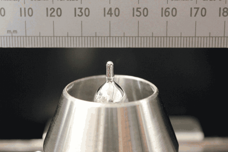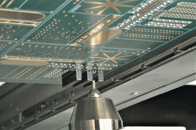
A micro nozzle is Pillarhouse’s patented 1,5 mm nozzle which helps to solve the challenges of particularly small nozzle requirements in selective soldering. The first challenge to overcome when designing the micro nozzle was the fact that the smaller the nozzle, the less thermal energy it has.

Before the micro nozzle was designed, the standard method of overcoming small nozzle requirements was to use a smaller standard nozzle design and then superheat the solder with an extremely high tip flow rate. One of the issues with this approach is that the temperature has a much smaller effect on the resulting heat transfer than flow rate. It also creates a situation where the process is susceptible to copper dissolution because of elevated solder temperature and dwell times. Additionally, an exaggerated flow rate at the tip was required to keep the solder from solidifying, so the advertised nozzle size is misrepresented, and the true contact area is much larger than the nozzle diameter would predict.
Pillarhouse’s solution is to provide a multi-section nozzle that enacts a solder flow rate internally equal to a nozzle 2,6 times as large, with a resulting tip flow equal to a standard design nozzle. This means the heat of the solder is refreshing the energy in the tip at a high rate, but the PCB is not exposed to the unsteady and vigorous flow.
The next patent involves the wettability of the nozzle itself and the ability to solder without bridging. Typically, the smaller the nozzle, the more quickly it will de-wet. This is a function of exposure time of the solder to O2 but mainly due to the small nozzle having less wetted area than the PCB wetted area (pads and leads). The rule of thumb is the greatest wetted area wins when trying to avoid bridging. The patent provides a design including external features on the tip itself that multiplies the surface area, much like corrugated cardboard has a greater surface area than flat paper. The result is a particularly small nozzle that has a strong ability to de-bridge fine and ultra-fine pitch components with enough thermal energy to solder multi-layer PCBs without extended dwell times, exaggerated contact flow or extremely high solder temperatures.

Heat/thermal energy
What are the advantages and disadvantages of heated nitrogen?
Heated nitrogen raises the environment temperature around the solder nozzle, requiring less energy to maintain temperature. As selective soldering nozzles do not have infinite thermal mass, this is important in reducing solder dwell times. Additionally, the heated nitrogen has an added benefit of locally heating a circuit board during the process which reduces the dwell times.
What are the advantages of heating nitrogen with a separate heat source?
Heating the nitrogen has diminishing returns once it exceeds the nozzle tip temperature. If the nitrogen provides energy to change the nozzle tip temperature, it is competing with the control on the heat source for the solder. The solder heat source has no ability to reduce temperature. Heated nitrogen can become another process variable that needs process control. Additionally, if you ‘superheat’ the nitrogen, you must be concerned about extended dwell times because it could potentially reflow SMT devices surrounding the target soldering area.
What are the main causes of copper dissolution solder temperature/dip time solder choice?
Alloy choice is particularly important in the copper dissolution scenario because lead-free alloys have a propensity to aggressively leach copper from the PCB. The downside of using an alloy that causes less copper dissolution is that it usually wets slower, making the process more difficult. For instance, SAC305 causes higher rates of copper dissolution than SN100C, but it is inverse in the dwell times required to solder, meaning extended dwell times and higher pot temperatures for the SN100C. The flow rate of the nozzle itself and the solder temperature/dwell time at contact also have a significant impact on copper dissolution.
Pump control
There are different pump styles currently on the market, including:
• Mixed-flow flat blade impeller mechanical.
• Mixed-flow impeller mechanical.
• Magnetic.
Pillarhouse uses both mixed-flow flat blade impeller mechanical, and magnetic pumps. Mechanical pumps provide higher resolution and better pump deceleration control for de-bridging fine pitch and PCBs with poor lead length. Mechanical pumps are rebuildable and have only nominally more dross per shift than magnetic pumps. Magnetic pumps have good solder acceleration and recovery, which is better for cycle time. There are no moving parts, the design is simple and has nominally less dross production than mechanical pumps.
Thermal calibration and its advantage over the mechanical method?
Thermal calibration is the single best process control in the Pillarhouse arsenal. The test confirms that not only are the XYZ axes working properly (contact out of place or wrong size otherwise), but it also shows that the nozzle is evenly wetted and the pump, solder level, and wave height are in control. By using thermal calibration, a customer can take a programme from another Pillarhouse system, recalibrate, and know the system will work the same as the previous machine, without wasting product. It is Pillarhouse’s belief that anyone can make a product work in a lab – the true test is when they have established a process and try the same product after six months with different nozzles and a new solder; can the system reproduce the same results?
| Tel: | +27 11 869 0049 |
| Email: | [email protected] |
| www: | www.mykaytronics.co.za |
| Articles: | More information and articles about MyKay Tronics |
© Technews Publishing (Pty) Ltd | All Rights Reserved