IoT products are demanding higher frequencies and wider bandwidths than ever with varied sectors driving the demand for extreme 5G speed support in RF PCB design. These include connected vehicles, smart homes, smart cities, connected health, smart media, smart agriculture, and smart industrial applications.
Compared to 4G, 5G networks can deliver up to ten times less latency with fifty times more speed and 1000 times more capacity making it the protocol of choice for new IoT designs and products. However, key challenges in RF PCB design need to be addressed like higher frequency and wider bandwidths, multiple input and multiple output (MIMO) and beam steering, over-the-air testing, and 5G NR’s coexistence with other wireless communication systems. These challenges are amplified as product complexity increases – products are demanding smaller form-factors while simultaneously housing larger circuits.
5G specifications stipulate that handsets must support four downlink paths for bands above 1 GHz, to enable higher data rates. This requires four antennas and four independent RF pathways. For many handsets, the change will mean a substantial increase in RF content, signal-routing complexity, and antenna bandwidth. It will be challenging to squeeze even more content into already-crowded space allocated to the RF front end, and highly integrated solutions will be needed to minimise solution size and increase performance.
Antenna tuning will become even more important to keep the total number of antennas within manageable limits. In addition, increased signal-routing complexity will require the use of antenna-plexers that maximise the number of signal connections, while maintaining low insertion loss.
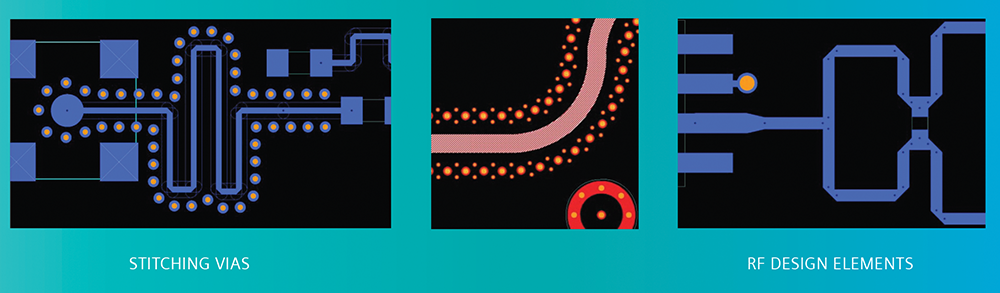
Companies wishing to take their design performance to the next level need to implement technology enablers to support their PCB design process, and designing PCBs with RF requires design features and capabilities that are specific to RF. These include:
• Ground stitching vias to shield RF circuits.
• Restrictive clearance rules specific to RF.
• Automated RF circuit arrangement and grouping.
• Meanders.
• Via-stitching for easy creation of co-planar wave guides.
• Flood regions with vias according to your rules.
• The import of complex RF shapes.
• Chamfered corners.
PCB design tools that support RF-centric design capabilities have a competitive advantage. Siemens Digital Industries Software provides you with a product design flow that puts your high-speed RF (IoT) products in a position to be ‘first-to-market’.
Potential risks of plasma treatment on PCBs MyKay Tronics
Editor's Choice
Plasma treatment involves exposing PCBs to an ionised gas, known as plasma, but despite many advantages, several risks must be managed to ensure safe and effective plasma application in EMS.
Read more...X-band radar RF Design
Editor's Choice Telecoms, Datacoms, Wireless, IoT
X-band radar systems, particularly those leveraging beamforming ICs (BFICs), advanced gallium nitride (GaN) and gallium arsenide (GaAs) components, are leading the way in providing the high-performance radar capabilities required for modern defence and surveillance.
Read more...LED driver for industrial power supply indication Altron Arrow
Editor's Choice Circuit & System Protection
A simple and small solution for driving an LED to provide visual feedback in the presence/absence of a system’s power using a chip not originally designed for this purpose.
Read more...MPLAB PICkit Basic ASIC Design Services
Design Automation
To make its robust programming and debugging capabilities accessible to a wider range of engineers, Microchip Technology has launched the MPLAB PICkit Basic in-circuit debugger.
Read more...Case Study: Siemens Valor automation solution ASIC Design Services
Editor's Choice Manufacturing / Production Technology, Hardware & Services
Electronics manufacturer BMK used Siemens Valor to enhance accuracy and speed up bill-of-materials quotations.
Read more...XJLink-PF40 JTAG controller ASIC Design Services
Test & Measurement
XJTAG, a specialist in electronic testing, has released its new XJLink-PF40 JTAG controller together with version 4 of its popular PCB software testing suite.


 printer friendly version