


The implementation of sensor networks is growing rapidly in a number of diverse fields including environmental monitoring, industrial IoT installations and home and building automation (HBA).
According to a January 2023 research report published by Spherical Insights & Consulting, the global wireless sensors market is expected to grow from USD 37 billion in 2021 to USD 149 billion by 2030, at a CAGR of 19%. There are many reasons for this growth, not the least of which is the sustainability movement which requires energy usage in buildings to be as efficient as possible. Smart sensor networks can monitor room occupation and usage, controlling heating, lighting and air quality automatically, even operating doors and windows.
In many situations it is desirable for sensors to be connected wirelessly in a mesh network. This saves infrastructure and cost since long cabling runs are not required. It also means that networks can be much more flexible since sensor nodes can be installed anywhere, including in remote and difficult-to-access locations.
However, the successful implementation of a wireless sensor network requires a mesh networking solution that has the following attributes:
• Low power: Individual sensor nodes must be self-sufficient, able to run on batteries, or using an energy-harvesting technology for many years without regular maintenance. Often, sensor nodes will be placed in locations where there is no accessible mains power. This is, of course, especially true for remote environmental monitors, but even in buildings, mains power may not be available, dependence on cables reduces the flexibility of a network and increases its cost, especially if hoists or ‘cherry-pickers’ become necessary.
• Scalable: There should be no effective limitation on the number of nodes in a network. As an enterprise expands, the network should be able to flex with it, updating the level of information provided.
• Easy to install: For a sensor network to be effective, it needs to be simple to install and be capable of being expanded without calling upon expert technicians.
One technology which addresses all these issues is NeoCortec’s NeoMesh wireless ad-hoc mesh networking system. NeoCortec believes that most existing networking technologies are based on methods related to IP protocols, an approach that is not best suited to wireless sensor networks. Instead, NeoMesh is a wireless protocol stack designed with versatility in mind, delivering ultra-scalable networks, without network managers, dramatically reducing power consumption. This is all based
on principles which are specifically optimised for this type of wireless sensor networks.
To better understand the advantages of NeoMesh, it is useful to compare it with legacy mesh network technologies that have limitations in terms of scalability and power efficiency. Legacy mesh networks are organised in a hierarchical system, where different nodes have different capabilities and functions within the network. A typical topology is illustrated below in Figure 1.
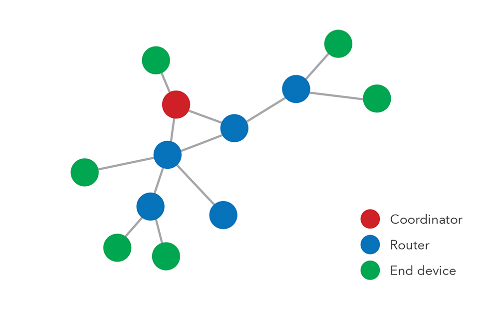 Figure 1. Legacy mesh topology.
Three types of nodes are visible:
1. The end device is the only part of this configuration that can be optimised for low power operation. Its sole function is to send and receive messages on its own behalf. It cannot route messages in the network, and therefore cannot be used to build the mesh network infrastructure.
2. The router can route messages through the network on behalf of other nodes. However, because a router must continuously listen for messages from end devices, which may transmit asynchronously, it will have a much higher power drain, and therefore cannot normally operate on batteries.
3. The coordinator is required to form and maintain the network, while also providing a central link to the Cloud or central server. The coordinator organises which nodes will be neighbours with which other nodes, and as such is a single point of failure. The coordinator cannot be battery powered.
Therefore, when selecting a wireless mesh network technology, it is vital to consider the entire power requirement. While individual nodes may be very low power, they require routers, controllers and uploaders – and sometimes extra cabling infrastructure - which will result in a much higher power budget than it first appeared on initial investigation.
The hierarchical structure of legacy mesh networks puts limitations on scalability as well as flexibility. The message routing principles of some mesh network topologies place severe restrictions on how the routing protocols handle deep network structures (for example, more than 10 hops) as well as dynamic configurations. These limitations reduce the deployment options, and effectively reduce the practical network size.
Decentralisation
In contrast, the NeoMesh network is decentralised (Figure 2). Instead of a master/slave configuration, all nodes are self-governing, all nodes act as routers, and nodes do not require a coordinator. This means that NeoMesh does not require different or ‘special’ node types, and all nodes share the same low power characteristics. This provides significant advantages over existing technologies in terms of power consumption for the entire network, with every node in the network running on small batteries for many years.
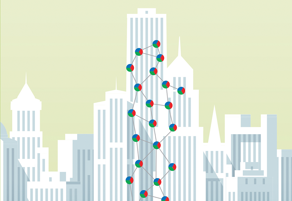 Figure 2. Decentralised NeoMesh network.
Moreover, the decentralised approach facilitates dynamic network topologies with no real limitation on scalability or network structures. These capabilities allow for full flexibility when deploying the network and allow for a network which scales with the application requirements. Expansion of a NeoMesh wireless mesh network is as simple as positioning a new node where required and switching it on. The other nodes in the existing system will ‘find’ the new node and incorporate it within the newly expanded structure.
Finally, the decentralised approach means that there is no central point of failure. If one node goes down for any reason, the system will ‘self-heal’ and find another route using other still-operational nodes for the information to be passed along. Data transmission through the network is done sequentially from node to node, until the data reaches its destination.
NeoMesh is ideally suited for wireless sensor networks where each sensor/device does not need to send data very often, and where the payload size is small. The NeoMesh wireless communication protocol is available in a series of fully integrated and pre-certified ultra-low-power bi-directional modules. Several versions of the modules are available; they all integrate the same core NeoMesh protocol stack across different frequency bands and come preloaded with the proprietary NeoCortec protocol stack.
| Tel: | +27 11 608 0070 |
| Email: | [email protected] |
| www: | www.cstelectronics.co.za |
| Articles: | More information and articles about CST Electronics |


© Technews Publishing (Pty) Ltd | All Rights Reserved
 printer friendly version