


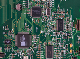
PCBs are essentially complex puzzles where the designer takes a specified list of components and a schematic diagram, typically with multiple sets of rules and constraints, then, following industry standards, guidelines, and best practices, places and connects them precisely for fabrication. Every step taken during the PCB design process is taken purposefully. Here are seven habits that highly efficient PCB designers have when completing their designs.
1. Efficient PCB designers pay attention to detail
Preparation is key, and it starts long before the PCB layout tool is launched. From building symbols and component land patterns from scratch, to obtaining them from tool libraries or online resources, PCB designers check them. Why? Because they can’t afford for them to be incorrect, no matter the source, since a single incorrect symbol or land pattern alone can result in a costly board respin.
Defining alternate package types for component and solder-side placement can save PCB real estate. Some surface-mount land patterns can even be optimised by including pre-defined breakout/fanout vias and thermal pads. An efficient designer will also identify opportunities to recommend schematic changes; for example, replacing individual resistors with a resistor network.
2. Efficient PCB designers study, plan, strategise, execute, and can regroup quickly
Efficient designers must become familiar with the schematic and think multiple steps ahead. Understanding a design’s schematic enables the designer to expedite placement. For example, defining groups or rooms of associated components, helps to expedite component placement. Understanding why and where discrete components, such as decoupling capacitors and bypass resistors, are needed on a board helps avoid signal and power integrity issues.
The ability to re-group and adjust quickly is critical for PCB designer efficiency, especially if a design’s release schedule is time-to-market critical. Efficient designers often create phased or daily backup versions of the design as part of their process, enabling them to easily revert to an earlier version if it expedites the update process. Efficient PCB designers are prepared for change, and they get better, smarter, and faster with every design completed.
3. Efficient PCB designers visualise
Component placement is a critical step and sets the stage for a successful PCB design layout. Component orientations, top or solder placement, and spacing that avoids shadowing and ensures optimal solderability and testing, are just a few of the details that designers are aware of, plan for, and visualise.
Efficient PCB designers visualise the design not only from a layout perspective, but also from a manufacturing perspective. They are aware that fabricators have their own internal processes and design rule checks. Details such as knowing which components require additional placement room during layout, perhaps driven with placement boundaries for example, can minimise or totally eliminate rework time after boards are fabricated.
4. Efficient PCB designers value working with, and consulting with, peers
Efficient PCB designers don’t work in a vacuum; they understand the value of collaboration. For example, early on they work closely with mechanical design teams to ensure the proper placement of mounting holes and physical interfaces such as connectors, LEDs, and displays. And, when problems are identified, they provide valuable feedback to the mechanical teams to improve the design. They think about the end product, embrace ECAD-MCAD collaboration, and keep the end product in mind throughout the PCB layout phase.
5. Efficient PCB designers strive for perfection
Getting a 95% in PCB design is not good enough. Even the smallest error, such as an incorrect pad size or a single trace that’s too close to a mounting hole, can result in a PCB re-spin. Efficient PCB designers do everything they can to achieve design perfection. From online design rule checks (DRC) and designing for manufacturing and assembly (DFMA) checks, every effort is made to ensure that the design work is accurate.
6. Efficient PCB designers continue to learn
Continuing education is a must in the electronic product design world. This includes keeping up with the latest industry standards including IPC, ANSI, MIL, etc., and in PCB fabrication and assembly processes. Technologies like the Internet of Things (IoT) and rigidflex circuits are becoming commonplace in today’s electronics, from automotive to medical, to consumer and beyond. PCB designers contend with a constant stream of new and improved components, packages, and fabrication, manufacturing, pre- and post-test and assembly processes as well.
PCB designers understand that they are not an island, but are rather part of a greater community of designers with a common goal. They subscribe to publications like PCD&F; and Circuits Assembly, are members of and/or regularly attend IPC chapter meetings and conferences, and may even present papers to peers at PCB conferences. Many PCB designers even seek industry credentials or certifications through training and testing like IPC’s Certified Interconnect Designer (CID) programme.
7. Efficient PCB designers’ designs reflect their passion
In as much as canvas is the medium to an artist, PC monitors are the virtual canvas for PCB designers. In fact, giving an identical design database to ten PCB designers is likely to result in ten different finished results. Perhaps the differences are subtle, or they might be visibly quite noticeable as each PCB designer has his or her own unique design style, where items that aren’t immutable or fixed can be tailored and unique.
Efficient PCB designers are passionate and meticulous about their work. It’s a job that requires a vast array of knowledge, skills, and attention to detail. Most importantly, they have a unique passion for electronics design. They enjoy the mental challenge, the sense of gratification, and the pride their contributions bring to the end products.
Conclusion
With the aid of electronic design CAD software, PCB designers both pilot and navigate each design aspect, applying their education and experience with the goal of first-pass design success. Developing design habits that expedite design completion, improve design quality, and enhance productivity are instrumental to highly efficient PCB design.
| Tel: | +27 11 315 8316 |
| Email: | [email protected] |
| www: | www.asic.co.za |
| Articles: | More information and articles about ASIC Design Services |


© Technews Publishing (Pty) Ltd | All Rights Reserved
 printer friendly version