
The Axcelerator family is a single-chip, nonvolatile FPGA solution that offers high densities, flexible I/Os, and unique logic to enable implementation of high performance, high gate count designs. Built on Actel's innovative sea-of-modules architecture on 0,15 µm antifuse process with seven layers of metal, Axcelerator FPGAs are designed to deliver pure performance with low power consumption, high logic utilisation, unprecedented design security and the world's fastest FPGA core.
New architecture
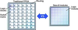
Based on the AX architecture, it builds on the evolution of Actel's sea-of-modules architecture. Axcelerator FPGAs have two basic modules, the C-cell (Combinatorial cell) and the R-cell (Register cell), which efficiently implement combinatorial and register-based logic. When combined, the R-cell and C-cell create Clusters. Two Clusters are then combined to form SuperClusters, which are organised into Core Tiles to make up a sea-of-modules at the chip level. The entire floor of the Axcelerator device is covered with a grid of logic modules with virtually no chip area lost to interconnect elements or routing (Figure 1).

Fast, hierarchical routing: Connecting the modules is a high-speed hierarchical routing structure. DirectConnects provide very high performance routing inside SuperClusters, while FastConnects provide high speed routing inside the SuperCluster and to the SuperCluster below. Additional CarryConnect routing connects C-cells in SuperClusters when building arithmetic functions. Core Tiles are also connected with vertical and horizontal routing resources. Finally, at the chip level, routing highways are used for efficient long-distance routing.

Performance: With seven layers of metal on a 0,15 µm process, the Axcelerator family was designed for speed and total logic utilisation. Redesigned flexible logic modules, highway tracks for carrying signals across the chip, extensive carry chain support, and many other innovative attributes have been implemented in the AX architecture to guarantee a high performance solution. Axcelerator FPGAs achieve better than 500 MHz internal and 350 MHz system performance.

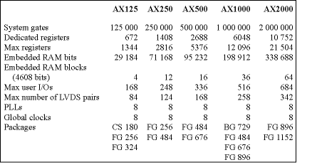
Density: Axcelerator FPGAs have densities ranging from 125 000 to 2 million equivalent system gates, making them well-suited for large, complex designs. With its abundance of interconnection resources, the innovative routing architecture exploits antifuse technology to achieve nearly 100% utilisation. With such high densities and utilisation, and low power consumption, Axcelerator FPGAs are a strong alternative to ASICs.
Flexibility: In addition to high performance and high density, Axcelerator FPGAs have numerous other features. Axcelerator FPGAs feature innovative SRAM/FIFO and PerPin FIFOs, enabling data to easily cross clock and phase domains. In addition, they have an integrated low-power mode to accommodate power-conscious designs, disabling one or more I/O banks while allowing operation of the device's internal logic. With flexible I/Os compliant with multiple standards, embedded SRAM with programmable FIFO logic, segmentable clock resources, and embedded PLLs, Axcelerator FPGAs have all the resources necessary for the complex designs of today and tomorrow.
Advantages
Using high performance FPGAs often means sacrificing other design goals. However, this is not so with Axcelerator FPGAs. Because these devices are antifuse-based, all the inherent benefits of antifuse technology apply. Since they are nonvolatile, they are live at power up so there is no latency issue while loading configuration data. Axcelerator also does not require a boot PROM, eliminating the possibility of intercepting configuration data. With the advanced AX antifuse architecture, Axcelerator FPGAs have the best performance-to-power consumption ratio of any FPGA and provide a secure, 'instant on' solution.
High security
FPGAs are quickly becoming the new alternative to ASICs. Many systems today have a significant portion of the total system-level IP inside the FPGA. Since a conventional SRAM-based FPGA is volatile, it must be re-initialised every time power is applied. This re-initialisation requires an external bitstream be loaded into the FPGA. This external bitstream also allows easy, non-invasive, copying of the design. Unlike SRAM-based FPGAs, Axcelerator does not require an external bitstream and provides significantly higher design security. The FuseLock secure programming technology used in the Axcelerator family is highly resistant to both invasive and non-invasive security attacks.
Multistandard I/Os
The Axcelerator family I/Os were designed with performance and flexibility in mind. The I/Os are bank-selectable with three registers per I/O. The I/Os are hot-swap compliant and support a range of mixed voltages and I/O standards (LVTTL, LVCMOS, 3,3 V PCI, 3,3 V PCI-X, LVPECL, LVDS, GTL+, HSTL Class 1, SSTL2 Class 1&2, and SSTL3 Class 1&2). In addition, each I/O features a 64-bit PerPin FIFO with a separate read and write clock.
The Axcelerator family provides the most flexible I/O structure of any FPGA. Each I/O features a 64-bit deep FIFO that can be independently controlled or combined for bus applications. The PerPin FIFO is unique to the AX architecture and can be used in conjunction with the 14 I/O standards offered by Axcelerator family devices. To further maximise flexibility, selectable, independent read and write clock polarities allow the transfer of data between different clock domains. Embedded I/O FIFO Controllers are provided so that 100% of the core logic resources are available to the user.

Embedded memory
Axcelerator devices have up to 64 blocks of embedded, variable-aspect-ratio SRAM with separate read and write ports that can be configured with different bit widths on each port. Configurations include 128x36, 256x18, 512x9, 1kx4, 2kx2, or 4kx1. Each SRAM block has an embedded FIFO control unit that allows the block to be configured as a synchronous FIFO with programmable flag generation. Each block also contains counters to generate address pointers and control circuitry to prevent metastability and error conditions.
Flexible clock
Axcelerator FPGAs have a number of clock resources available to the designer. Every device contains four hardwired and four routed clocks. In addition, every device has a global preset/clear signal available. Each hardwired and routed clock has an associated analog PLL. These eight PLLs can operate with input frequencies from 14-200 MHz and can generate output frequencies between 20 MHz and 1 GHz.
ASIC Design Services is holding Programmable Logic Seminars in April - see 'Events'. For information contact Kobus van Rooyen, 011 315 8316.
| Tel: | +27 11 315 8316 |
| Email: | [email protected] |
| www: | www.asic.co.za |
| Articles: | More information and articles about ASIC Design Services |

© Technews Publishing (Pty) Ltd | All Rights Reserved