
For nearly a decade, Actel FPGAs have been successfully deployed in flight-critical applications in space. In fact, having been used on many major European Space programmes in the past, they are now an essential component on virtually all new programmes. Their flexibility and reliability make them ideal devices for implementing numerous functions on both platform and payload.
Nevertheless, until recently, the available gate count for space-qualified families has limited their use to less complex functions. These functions are typically within the platform part of the satellite, or simple payload applications. However, for the large, more complex functions that are more typical of payloads, designers have had no practical alternative to ASICs, with their high NRE and long development timescales. Now, new process technology, and a new radiation-tolerant register cell have produced an FPGA family that dramatically increases the size of design which can be implemented for space applications, bringing the cost and time-to-market benefits of FPGAs to a significantly wider range of projects.
The SX-S family has been specifically developed by Actel to meet the needs of designers of space applications. By increasing the number of available gates, at the same time as removing the need to add logic redundancy, design complexity can be increased up to 6-fold over previous generations. This article describes the technology behind this development, and illustrates how it combines with the established anti-fuse FPGA benefits of high reliability, latch-up immunity, deterministic power-up, high flexibility and swift design cycles, to provide an attractive alternative to ASICs in space designs up to 40k ASIC gates.
Radiation hardened flip-flops - the key to efficient system design
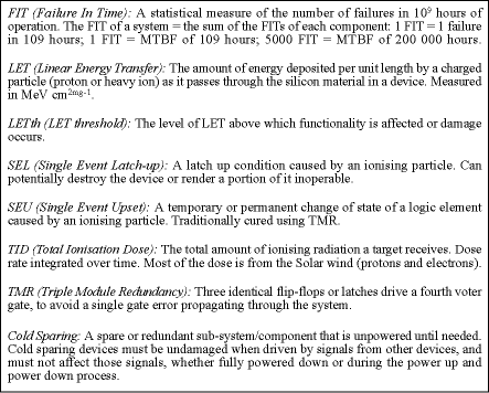
The radiation environment in space presents three main challenges, Single Event Latch-up (SEL), Total Ionisation Dose (TID) and Single Event Upset (SEU) (Table 1 describes some basic terminology). In common with other Actel space FPGAs, the SX-S is immune to SEL (threshold > 105 MeV/gm/cm2), while TID performance is >100 krad. As far as SEU is concerned, it is well understood that as geometries shrink, susceptibility increases, and to withstand SEU, designers have traditionally needed to implement redundancy and voting regimes, for example TMR. This means that a space design has required two to four times the gate count of an equivalent non-space design, limiting the design complexity that can be implemented on a given device. The key element in developing a family specifically for space applications, therefore, was the creation of a register cell that is immune to SEU, and consequently does not require this redundancy.
Building on the proven SX-A family of anti-fuse FPGAs, the new SX-S provides combinational C-Cells and R-cell registers in a 'sea of modules' architecture. While the 'sea of modules' architecture combined with four layer metal (three layer for the smallest die size) maximises logic area for a given die size, the main development effort has been focused on modifying the R-cell of the SX-A to withstand a stringent SEU requirement of a LETth greater than 60 MeV/gm/cm2, without altering its functionality. This criterion exceeds the generally accepted threshold to be considered immune to SEU, which is 38 MeV/gm/cm2. Since this means the SX-S is immune to SEU, engineers no longer need to trade-off SEU immunity using TMR against efficient use of logic real estate. What you see is what you get, especially when supported by 100% circuit resource utilisation. By designing a new cell structure, Actel has also been able to implement the hardened registers in such a way as to avoid the problems that can affect 'soft' TMR registers implemented in user-routed conventional cells. The new hardened flip-flop is fast, and does not glitch on its output.

A new SEU-hardened cell structure
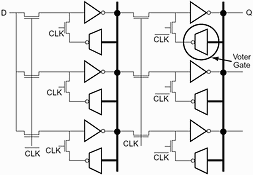
Both the Master and Slave latches of each SEU-hardened R-cell are implemented using three latches, with the local feedback loop of each latch completed through a voter, which is also fed from each of the other two latches. If one of the three latches is hit by a charged particle and changes state, the voting from the other two latches prevents the change from feeding back and appearing on the output. Careful layout ensures that a single ion cannot affect more than one latch. Simplified representations of both a conventional R-cell and the SEU-hardened SX-S R-cell are shown in Figure 1 and Figure 2.
To provide for the necessary quality control, the R-cell of the SX-S family includes additional test circuitry, which enables extensive testing of each individual latch and voting circuit during wafer sorting, final test and post burn-in test of the unprogrammed devices. Once the device is programmed, this test circuitry is disabled.

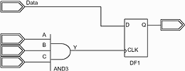
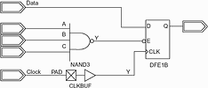
Bearing in mind the need to achieve reliable designs with minimum design time, the R-cell also includes several features intended to simplify good design practice, and increase flexibility. For example, the inclusion of clock enable facilities simplifies the implementation of fully synchronous designs, avoiding the glitch-prone use of combinational logic on clock pins either to implement an enable function, or to generate local clocks. See Figures 3-6. Not only does a fully synchronous design methodology greatly simplify and speed-up designs, since only static timing analysis is required, but also it offers other benefits during system prototyping. Because the R-cell has been redesigned for the SX-S, there are some detailed timing differences to commercial SX registers, but they have identical functionality, so it is possible to test prototype fully synchronous designs using lower cost non-space parts, and then replace with pin-for-pin compatible SX-S space parts for flight use.
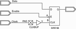

Table 2 summarises how this new cell performance translates into device performance, based on the radiation environment of a typical geostationary orbit (GEO orbit, 100 mil Al shielding and Solar min). Critically, the table not only considers the resulting bit upset rate (upsets per bit per day), but also the device upset rate. Since device upset rate = bit upset rate x bit count, the significantly higher bit density of SRAM-based FPGAs (composed primarily of its configuration SRAM), compared to anti-fuse topology of the same gate count, results in much higher device upset rates, even when the bit upset rate is similar. Note that the new SX-S device delivers a 104 improvement in device upset rates even over previous generations of Actel FPGA.
Proven suitability for space
Actel's proven anti-fuse technology provides a number of intrinsic benefits for space applications, which are naturally continued within the SX-S family. Because there is no program to load, the devices are live at power-up, and require no special power supply sequencing, which can significantly simplify system design. The devices can also be used in Cold Sparing applications, where redundant logic is only powered up when required (for example if problems are detected elsewhere in the system). For the rest of the time they can remain powered down within the 'live' system. This is achieved because the I/Os of the powered down device remain in a tri-stated condition, ensuring that the device is not damaged, nor are there any effects on the external signals from other, powered, devices. Optional pull-up or pull-down resistors may be enabled during power-up, in order to put undriven buses into a known state during this time.
The I/O is extremely versatile, and may be configured to support 3,3 V/5,0 V PCI, LVTTL, TTL and CMOS (including 5,0 V CMOS trip levels), as well as supporting mixed 3,3/5,0 V operation, making the SX-S ideally suited to interfacing with, and controlling, a wide range of peripheral devices and technologies.
Major benefits over ASICs
The relatively low volumes normally required for space applications are clearly ideal for FPGAs, and despite the long project timescales of typical projects, the fast turn-round of FPGA programming enables design iterations to be continued later in the project, providing the flexibility to accommodate changing mission priorities or to meet modified requirements.
Because every design uses the same FPGA part, the collection of vital data such as TID and FIT data is also much more practical, and therefore more extensive than for ASICs, where every design is a new part. Similarly, while ASICs typically achieve around 50-100 FIT, the Actel anti-fuse families range from 6-20 FIT, giving five to 10 times the reliability.
Quality is vital
In addition to full QML certification to the MIL-PRF-38535-compliant quality management procedures, processes and controls, SX-S devices are supplied from TM1019.5-tested pedigreed lots. TID data is available for each lot, listing both functional and parametric data ( www.actel.com/hirel).
The SX-S devices have extensive test circuitry built into them, which allows production testing of all internal logic (R and C modules), together with all I/O, interconnect, by-pass transistors and anti-fuses. In addition, the SX-S devices support IEEE 1149.1 JTAG Boundary Scan testing, with a dedicated JTAG Reset being available. Development is speeded up by Actel's unique Silicon Explorer II debugger, which allows realtime access to any two internal nodes within the FPGA. These are displayed on a fully functional, 18 channel PC-based logic analyser, together with up to 16 system-level signals to enable design verification to take place at the engineer's desk. A security fuse ensures that after verification, the Intellectual Property (IP) of the design is immune from investigation.
The practical alternative
The low quantity, and high reliability demands of space are an ideal fit for anti-fuse FPGA technology, leading to widespread use of previous generations of devices. More than a decade of working with space designers has enabled Actel to create a new family especially for these applications, focusing on simplifying the design task through developing a radiation hardened register cell. At the same time, utilising a 0,25 µm process and 'sea of modules' architecture has transformed the amount of logic available in each device.
For the largest designs, project engineers may still be forced to accept the significant NRE and delivery penalties of using an ASIC. However, with up to 6 times the number of gates available in the SX-S family, the proven flight-critical reliability and low cost of FPGAs is now a practical alternative for payload designs and complex platform sub-systems up to 40k ASIC gates.
For more information contact Kobus van Rooyen, ASIC Design Services, 011 315 8316.
| Tel: | +27 11 315 8316 |
| Email: | [email protected] |
| www: | www.asic.co.za |
| Articles: | More information and articles about ASIC Design Services |

© Technews Publishing (Pty) Ltd | All Rights Reserved