Isolation between circuit components is typically required for safety and/or data integrity considerations.
For example, isolation protects sensitive circuit components and human interface on the system side from dangerous voltage levels present on the field side, where more robust components such as sensors and actuators reside. Isolation can also eliminate common mode noises or ground loops that affect data acquisition accuracy.
While data transfer across an isolation barrier can be achieved through traditional opto-couplers or Analog Devices' iCouplers, the main challenge and common headache has been to find a way to transmit power from the non-isolated system side to the isolated field side. This article discusses the technology behind a new approach and addresses this challenge by integrating power supply isolation with data signal isolation using Analog Devices' latest iCoupler products.
Until recently, transferring power across an isolation barrier required either a separate DC-DC converter, which is relatively large, expensive and has insufficient isolation, or a custom discrete approach, which is not only bulky but also difficult to design and interface. These approaches have been the only viable alternatives, even in applications such as data acquisition modules where only small levels of isolated power are needed.
Analog Devices has recently addressed this issue with the introduction of a complete and fully integrated isolation solution involving signal and power transfer across an isolation barrier using micro-transformers. This extension to our iCoupler technology, termed isoPower, is a breakthrough alternative. Signal and power within a single component, eliminates the need for a bulky, expensive, difficult to design isolated power supply and provides adequate isolation up to 5 kV. It can significantly reduce the total isolation system cost, the board space and design time. A two channel iCoupler device with isoPower as shown in Figure 1 is almost 90% smaller and 70% less expensive.

iCoupler technology with isoPower
The integration of DC-DC converters involves the use of transformer switches, rectification diodes and most importantly, a transformer. Reducing the size of the transformer to enable its integration in a complete isolation solution is made possible by using high switching frequencies, on the order of 300 MHz. This runs counter to the approach used in magnetic core transformers where the permeability of the magnetic core starts to degrade at high frequencies, leading to appreciable core loss that lowers efficiency. In addition, a magnetic core could also compromise the isolation rating of the transformers. Coreless iCoupler transformers, on the other hand, can be switched at higher frequencies and are much simpler to implement.
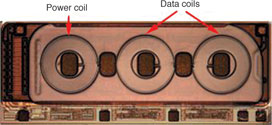
The micro-transformers used in iCoupler devices are built on top of a CMOS substrate. Figure 2 shows a cross-section of the isolated transformer structure, and Figure 3 is a die photo with both power and signal transformers. The transformer series resistance is minimised through the use of 6 µm thick plated gold for both the primary and the secondary spirals. The 20 μm thick polyimide in between the primary and the secondary provides HV isolation up to 5 kV. The additional 5 μm thick polyimide under the bottom spiral helps to reduce substrate capacitance and substrate loss. The substrate loss is further reduced through carefully designed patterned ground shield, using available underlying IC metal. The proximity effect and eddy current loss is less of a concern for the stacked transformers with large magnetic coupling coefficient. The design of the coils can be done through the optimisation of coil parameters, such as the number of turns, trace width and trace pitch. The quality factor (Q) at 300 MHz can be as high as 20 for the top coil and 15 for the bottom coil. The high Q for the micro-transformer structure makes an efficient power transfer possible.


The transfer of the digital signal is realised through transmitting short pulses (around 1 ns wide) across the transformers with two consecutive short pulses to indicate a leading edge and a single short pulse as a falling edge. Figure 4 shows the signal transfer block diagram. A non-retriggerable monostable at the secondary generates detection pulses. If two pulses are detected, the output is set to High. On the other hand, if a single pulse is detected, the output is set to Low. An input filter helps to increase noise immunity. The DC correctness is guaranteed by refresh signals sent into the transformers when no signal edges are detected for about 1 µs. If the input is high, two consecutive short pulses are generated as refresh pulses and if the input is low, refresh of a single short pulse is generated. To complement the refresh circuit on the driver side, a watchdog is implemented in the receiver to make sure the output is at a fail-safe state when no refresh pulses are detected.

Similar micro-transformers are used to transfer power. Because of their small L/R ratio, the transformers need to be switched at a high frequency to avoid current saturation and to achieve high efficiency. An example of four complementary CMOS switches implemented in a cross-coupled configuration, together with the transformer forming sustaining oscillation, is shown in Figure 5. The tank component sizes are optimised to maximise the energy transfer efficiency. The integrated Schottky diodes were used as rectification devices. These diodes turn on and recover fast enough for 300 MHz rectification. The diodes need to be sized such that they stay in Schottky region during rectification. A linear regulator on the secondary maintains the output voltage with output load or input supply variations. Efficiency is less of a concern for many low power applications. To improve efficiency and maintain energy regulation, an optional feedback signal transformer can be added. The feedback signal would turn on/off the LC tank instead of controlling the transformer switches directly. This approach essentially separates the energy regulation from energy conversion allowing optimised power transfer and maintaining regulation.

One common concern about switching transformers is their electromagnetic interference, particularly for a transformer switching at 300 MHz. Using the far-field approximation;
P = 160 π6 I² Σ (rn/λ)4; n = 1,2,...,N
where:
P = total radiated power
I = coil loop current
The wavelength, λ at 300 MHz is about 1 metre, the transformer with a radius in the range of 0,5 mm is still a very poor antenna with a small r/λ. It is estimated that the total radiated power is still less than 500 pW even if the part is operating at 300 MHz with a loop current of 350 mA. The near field radiation drops rapidly with the distance from the transformer. The on-chip transformers are only closely coupled with a small separation, 20 μm in our case.
Example application: The ADuM5242 in a secondary control power supply
Secondary control architectures have gained traction as new power supplies trend toward lower supply voltage, faster dynamic response and more system interaction between the supply and the load. There are two main difficulties in adopting secondary control versus primary control. The first is the need of high performance digital isolation versus analog isolation. An inexpensive analog opto-coupler is typically used to send analog feedback error signal from the secondary to the primary in a system with primary control while an expensive or bulky digital coupler would be needed to send PWM signals across the isolation barrier for a system with secondary control.
The second difficulty is the need for power at the secondary controller before the system has started up. The primary controller has no such issue as power is always available at the primary side. There are mainly two ways to solve this secondary control start-up issue. One method is to add an auxiliary power supply exclusively for the secondary controller start-up. A second method is to have a dedicated start-up component on the primary side to build initial bias at the secondary for the start up of secondary controller.
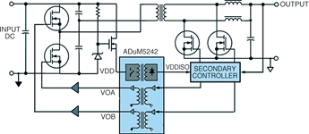
Analog Devices' ADuM5242, a dual channel digital isolator with a 50 mW isolated output is an ideal solution to the startup problem. This 8-lead SOIC component provides two isolation channels that support PWM signals up to 10 Mbps and 10 mA of 5 V isolated power for the start up of the secondary controller. The user has further option to disable the power once the system is started up. The disable is achieved through monitoring the input supply voltage. When the input supply drops below 4 V the feedback control switch shown in Figure 5 is turned off. Figure 6 is an example application block diagram for the use of ADuM5242 in a secondary control system. The two digital signal channels provide the feedback signals from the secondary controller with synchronous rectification to drive the half-bridge drivers at the primary.

Together with ADuM5242, two other data channel configurations have also been introduced. The ADuM5240 has two isolated output channels while the ADuM5241 has one isolated output and one isolated input. This provides the flexibility to support a wide variety of applications. The ADuM524x products can also be used in combination with other multichannel iCoupler devices to configure higher quantities of isolated signal channels.
Summary
iCoupler technology with isoPower provides a complete isolation solution within a single package. Not only does it offer state-of-the-art digital signal isolation having substantial advantages over opto-couplers in terms of power, size and performance, but it also eliminates the need for a separate, isolated power supply. The iCoupler technology provides unprecedented possibilities for functional integration that can dramatically reduce the complexity, size and total cost of the isolated systems.
© Technews Publishing (Pty) Ltd | All Rights Reserved