Over the past decade, field-programmable gate arrays (FPGAs) have achieved widespread adoption across an expanding array of applications. By offering a universal silicon platform that can be quickly programmed for a specific application and reprogrammed with each iteration of a design, these highly flexible devices have quickly become an essential prototyping tool for many design teams and have frequently been used in low- to medium-volume applications.
Despite this success, however, FPGAs have yet to achieve widespread adoption in high-volume applications. When engineers are ready to migrate designs to higher volume production levels, standard cell-based application-specific integrated circuits (ASICs) have typically offered the lowest cost alternative. ASIC technology's low unit cost, high performance, and low power consumption have proved formidable advantages in these higher volume environments. But as ASIC manufacturers have migrated to subquarter-micron process technologies and non-recurring expenses (NREs) have rapidly increased, those traditional cost advantages have evaporated.
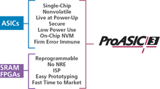
Today, by leveraging the advantages of the latest semiconductor processes and using innovative architectures, FPGAs not only offer unit costs comparable to traditional ASICs, but match or exceed many of the power, security, reliability, live-at-power-up, and performance advantages historically accorded only to ASICs (Figure 1).

Fabricated with Flash technology, the Actel Flash-based ProASIC3/E devices are the first FPGAs to deliver all of these capabilities. ProASIC3/E devices offer designers a secure, high-performance, low power, programmable, single-chip solution that is live at power-up, and available at ASIC-like price points.
What do designers look for in a 'production FPGA'? The ideal silicon solution would offer the following seven basic features:
* Single-chip.
* Affordable integration of multiple system functions with no NRE costs.
* Live at power-up.
* Intellectual property (IP) security.
* Low power.
* Reprogrammable and customisable.
* Rapid time-to-market.
Cost-optimised architecture
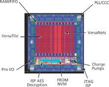
To achieve the ideal silicon solution, Actel's ProASIC3/E product line employs a proprietary architecture comprised of the following components (Figure 2):

* FPGA VersaTiles: Each VersaTile can be configured as a three-input logic function or a D-flip-flop or latch by programming the appropriate Flash switch interconnections. VersaTiles support a higher utilisation rate than comparable SRAM FPGA cells due to the flexibility of their usage as a register or latch.
* Dedicated FlashROM (FROM) nonvolatile memory: a primary distinction between SRAM-based FPGAs and Actel ProASIC3/E FPGA technology is the addition of 1024 bits of dedicated nonvolatile FROM memory on each device.
* Dedicated SRAM/FIFO memory: extensive memory resources can be used as either RAM or FIFO.
* Extensive clock conditioning circuitry (CCC) and phase-locked loop (PLL) features.
* Pro I/O structure: high I/O counts per number of system gates allows designers to implement I/O-intensive designs without moving to higher-density devices.
* FPGA VersaNet globals.
* JTAG ISP/UJTAG port.
* AES decryption mechanism.
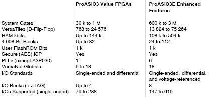
Lower density devices in the product family address the 'value' FPGA market segment, while the higher density parts are targeted at applications requiring a full-featured FPGA. For the value-based FPGA market segment, the ProASIC3 devices offer extended logic density and I/Os. Most devices have support for additional I/O standards, SRAM, and a PLL. For higher end applications, the PA3 product line adds enhanced features such as high-density logic, SRAM and I/Os, advanced I/O standards, and up to six PLLs (Table 1).

Flash technology
The key to these density, performance, and security improvements over traditional SRAM-based FPGAs is the use of an advanced Flash-based LVCMOS process with seven metal layers. Standard CMOS design techniques are used to implement logic and control functions. The combination of fine granularity, enhanced flexible routing resources, and abundant Flash switches allows for industry-leading, high logic utilisation without compromising device routability or performance.
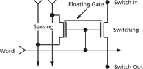
The ProASIC3/E Flash-based FPGA devices are based on a Flash programming element that uses a two-transistor structure (Figure 3).

Flash switches are distributed throughout the device to provide nonvolatile, reconfigurable interconnect programming. Unlike SRAM-based FPGAs that often fail to place-and-route at approximately 70% utilisation, maximum core utilisation is possible for virtually any design in the Flash FPGA architecture. In addition, extensive on-chip programming circuitry allows for rapid (3,3 V) single-voltage programming of the ProASIC3/E devices via an IEEE1532 JTAG interface.
This structure differs from SRAM-based FPGAs that require four to six transistors to make a single programming element. This difference carries significant advantage when comparing die area of the devices. In a given process, FPGAs based on a Flash programming element will be smaller than the SRAM FPGAs. As a result, SRAM-based FPGAs must be fabricated on a smaller, more expensive and power-hungry process technology to offer a comparable cost.
The use of Flash technology as the foundation for the ProASIC3/E devices offers a number of additional advantages over traditional SRAM-based FPGAs, including lower system cost due to fewer external components, availability of user nonvolatile memory, higher levels of security, lower power consumption, live-at-power-up capability, and firm-error immunity.
Design tools
Actel offers extensive support for ProcASIC3/E in the Libero IDE and Designer FPGA development software tools to help the user implement an effective design quickly. The Actel Libero IDE is an integrated design manager that seamlessly integrates design tools while guiding the user through the design flow, managing all design and log files, and passing necessary design data among tools. Additionally, it allows users to integrate both schematic and HDL synthesis into a single flow and verify the entire design.
Summary
To address today's rapidly shortening product life cycles, shrinking time-to-market windows, and relentless cost pressures, designers need a silicon solution that provides the flexibility and fast turnaround capabilities traditionally associated with FPGAs. Actel ProASIC3/E Flash devices combine the best from both the ASIC and FPGA worlds. By bringing together in a single chip a programmable platform that offers low unit costs, low power, live-at-power-up capability, high levels of security, and firm-error immunity, Actel offers designers the first production FPGAs capable of lowering total system costs and accelerating development in high-volume applications.
| Tel: | +27 11 315 8316 |
| Email: | [email protected] |
| www: | www.asic.co.za |
| Articles: | More information and articles about ASIC Design Services |

© Technews Publishing (Pty) Ltd | All Rights Reserved