The SmartFusion 2 system-on-chip (SoC) FPGA is differentiated from other FPGAs by its low power capabilities that enable orders of magnitude lower power operation in low duty cycle applications.

The device family includes the following important low power features:
* The industry’s lowest static power.
* Flash*Freeze real-time low power state.
* ARM Cortex-M3 low power modes.
* SoC peripheral low power modes.
In systems that operate reactively or periodically, SmartFusion2 FPGAs can dramatically reduce power. Reactive operation is defined as a standby state waiting for some activity or event before processing is initiated. The reactive system returns to the standby state after processing is complete. Examples of reactive systems include a patient health monitor alarm that is activated when a patient falls down and a remote sensor initiating communication after detection of an event.
Periodic operation is defined as activity that must be performed on a recurring basis. These systems perform some processing and then enter standby mode. At a fixed time interval, the system repeats the processing function and returns to standby mode. Examples of periodic systems are standard wireless protocols, heart rate monitors that measure the pulse pressure periodically and remote sensors periodically picking up information.
Energy is saved in periodic and reactive systems by moving into a very low power state when processing is not necessary. This is possible within SmartFusion2 FPGAs using the ARM Cortex-M3 low power modes and Flash*Freeze mode in the FPGA fabric and I/Os. The capabilities of Flash*Freeze mode, however, are completely unique in FPGAs.
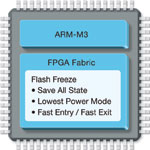
Flash*Freeze technology enables the rapid stopping and starting of the FPGA fabric and related I/Os while preserving the state of the FPGA fabric and dramatically reducing power. The time to either enter or exit Flash*Freeze mode is approximately 100 s.
While in Flash*Freeze mode, the state of the FPGA is maintained so that upon exit the device continues to operate where it left off.
Flash*Freeze operation
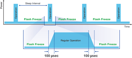
Figure 2 shows an example of Flash*Freeze operation with a 10 ms duty cycle, as used by commercial 3G Wideband Code Division Multiple Access (W-CDMA) based wireless communication. In W-CDMA systems when the phone is in standby mode, specialised circuitry wakes up every 10 ms and listens for a random access channel (RACH) signal, which indicates an incoming call. When no call is detected, the circuitry goes back to sleep, significantly saving battery life.

In Figure 3, the total ‘on’ time is 300 s plus 100 s to exit Flash*Freeze mode, and another 100 s to enter Flash*Freeze mode. For the other 9,5 ms of the period, the FPGA is in Flash*Freeze mode, consuming very little power. During the ‘on’ time of 300 s, the SmartFusion2 device is capable of processing about 50 000 M3 instructions and executing 50 000 FPGA clock cycles, including 10 million multiply-accumulate operations (a clock frequency of 166 MHz is assumed for Cortex-M3 processor, FPGA fabric and Ethernet MACs).

In this example, the resulting power reduction for the FPGA is an additional 20 times over a device that does not have Flash*Freeze capability.
The options for Flash*Freeze mode include the following:
* Saving state of memories.
* Keeping select PLLs turned on.
* Identifying which I/Os stay active.
* Defining what triggers the device to exit Flash*Freeze mode.
Triggering Flash*Freeze exit
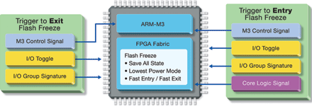
Exiting Flash*Freeze mode can be initiated through I/Os or through the Cortex-M3 processor. These methods send a message to the system controller to begin Flash*Freeze exit. Using I/Os to trigger Flash*Freeze exit can be done with Signature mode or Activity mode settings.
In Signature mode, a selected set of I/Os is configured as inputs with predetermined 1 and 0 comparison states. When the input signals for all the Signature mode I/Os match their predetermined 1 and 0 states, the system will initiate Flash*Freeze exit. All I/Os in Signature mode are compared as a single signature.
In Activity mode, a selected set of I/Os are configured as inputs and any change on any of the inputs will initiate Flash*Freeze exit. The device can be also have a combination of one group of Signature mode inputs and a set of Activity mode inputs, either of which can initiate Flash*Freeze exit.
The Cortex-M3 processor can initiate Flash*Freeze exit through a communication to the system controller through the comm port.
See Figure 4.

Initiating Flash*Freeze entry
Flash*Freeze low power mode can be initiated from the Cortex-M3 processor, the I/Os, or a core logic signal in the FPGA fabric. This flexibility includes all the capabilities for exiting Flash*Freeze mode, but also adds the FPGA fabric as an additional method. Using the FPGA fabric, nearly any desired complex event or state can initiate Flash*Freeze low power mode.
Security with Flash*Freeze mode
All methods of entering and exiting Flash*Freeze mode are controlled by the user during the design. In secure systems, all methods of entering and exiting Flash*Freeze mode should be controlled from within the FPGA and M3, and should not utilise any external signalling. This keeps external attackers from utilising Flash*Freeze mode to disable the system.
Flash*Freeze mode can also be used within security systems as a punishment where several pass-key checks have failed – similar to smartphone time-out when too many password entries have failed. This is one method of dramatically decreasing the number of pass-key attacks that can be performed on a system, thus mitigating brute force attacks.
Flash*Freeze applications
Communications
In low power communication systems, power is reduced by using periodic bursts of communication. This eliminates the constant power in the amplifiers and the rest of the system.
Sensor networks
Sensor networks include both low power communications and active sensors to perform distributed measurements. The active sensors can be turned on periodically (traffic image, weather sensor) or can turn on in response to an event (earthquake). After the measurement has been taken, the information is uploaded as an information burst and then the equipment goes back to sleep – in Flash*Freeze mode.
Medical equipment
Many types of medical equipment are used for monitoring patient health. These have relatively low sampling rates and can therefore utilise periodic operation as a means to minimise power consumption. This is especially useful in portable medical equipment.
SmartFusion2 Power Savings
SmartFusion2 SoC FPGAs implement power saving modes in the ARM Cortex-M3 processor and SoC peripherals. The Cortex-M3 core has Sleep and Deep Sleep modes that allow the device to be put into a low power state.
Sleep mode stops the processor clock to reduce power consumption, and Deep Sleep mode also stops the processor PLLs and Flash memory. The SoC peripherals can be shut down individually if they are not used in a design in order to reduce power consumption further.
SmartFusion2 SoC FPGAs have several ways to lower power consumption, ranging from their power saving modes to the power saving benefits of using a Flash memory architecture. In Flash*Freeze mode, the FPGA fabric consumes only 1 mW and takes no more than about 100 s to enter or exit.
The static power of a 50K gate SmartFusion2 device is 10 mW, a fraction of the leakage current of a comparable SRAM-based FPGA. Independent of these features, the processor core and the SoC peripherals can be put into low power states if required.
Being the lowest power SoC FPGAs with an integrated ARM Cortex-M3 processor, SmartFusion2 devices are ideal for use in any power sensitive application in the industrial, medical, military, avionics and communication markets.
| Tel: | +27 11 315 8316 |
| Email: | [email protected] |
| www: | www.asic.co.za |
| Articles: | More information and articles about ASIC Design Services |

© Technews Publishing (Pty) Ltd | All Rights Reserved