
Editor’s note: The following is the second part of an article series from Analog Devices covering time-of-flight system design. For a broad system overview, browse to www.dataweek.co.za/*aug21-adi to be redirected to Part 1 on Analog Devices’ website.
Time-of-flight (ToF) is an emerging 3D sensing and imaging technology that has found numerous applications in areas such as autonomous vehicles, virtual and augmented reality, feature identification and object dimensioning. ToF cameras acquire depth images by measuring the time it takes the light to travel from a light source to objects in the scene and back to the pixel array.
The specific type of technology that Analog Devices’ ADSD3100 backside illuminated (BSI) CMOS sensor implements is called continuous wave (CW) modulation, which is an indirect ToF sensing method. In a CW ToF camera, the light from an amplitude-modulated light source is backscattered by objects in the camera’s field of view (FOV) and the phase shift between the emitted waveform and the reflected waveform is measured.
By measuring the phase shift at multiple modulation frequencies, one can calculate a depth value for each pixel. The phase shift is obtained by measuring the correlation between the emitted waveform and the received waveform at different relative delays using in-pixel photon mixing demodulation. The concept of CW ToF is shown in Figure 1.

Depth sensing optical system architecture
Figure 2 shows the optical system architecture. It can be broken down into two main sub-module categories: imaging module (also known as receiver or Rx) and illumination module (also known as transmitter or Tx). The following sections introduce the function of each component, requirements distinct to the ToF system and corresponding design examples.
Illumination module
The illumination module consists of a light source, a driver that drives the light source at a high modulation frequency and a diffuser that projects the optical beam from the light source to the designed field of illumination (FOI), as illustrated in Figure 2.

Light source and driver
ToF modules normally use light sources that are narrowband with low temperature dependence of the wavelength, including vertical cavity surface emitting lasers (VCSELs) and edge emitting lasers (EELs).
Light emitting diodes (LEDs) are generally too slow for ToF modulation requirements. VCSELs have gained more popularity over recent years due to their lower cost, form factor and reliability, along with being easy to integrate into ToF modules. Compared with EELs (that emit from the side) and LEDs (that emit from the sides and top), VCSELs emit beams perpendicular to their surface, which offers better yield in production and lower fabrication cost. In addition, the desired FOI can be achieved by using a single engineered diffuser with the designed divergence and optical profile. The optimisation of the laser driver, as well as the electrical design and layout of the printed circuit boards (PCBs) and light source are critically important to achieve high modulation contrast and high optical power.
Illumination wavelength (850 nm vs. 940 nm)
While the ToF operational principle does not depend on the wavelength (rather it depends on the speed of light) and therefore the wavelength should not affect the accuracy, the choice of wavelength can affect the system-level performance in some use cases. The following are some considerations when choosing the wavelength.
Sensor quantum efficiency and responsivity
Quantum efficiency (QE) and responsivity (R) are linked to each other.
• QE measures the ability of a photodetector to convert photons into electrons:

• R measures the ability of a photodetector to convert optical power into electric current:

where q is electron charge, h is Planck’s constant, c is the speed of light, and λ is wavelength.
Typically, the QE of silicon-based sensors is about two times (or more) better at 850 nm than at 940 nm. For example, Analog Devices’ CW ToF sensors have 44% QE at 850&nbs;nm and 27% QE at 940 nm. For the same amount of illumination optical power, higher QE and R lead to better signal-to-noise ratio (SNR), especially when not much light returns to the sensor (which is the case for faraway or low-reflectivity objects).
Human perception
While the human eye is insensitive in the near infrared (NIR) wavelength range, light at 850 nm can be perceived by the human eye. On the other hand, 940 nm is invisible to the human eye.
Sunlight
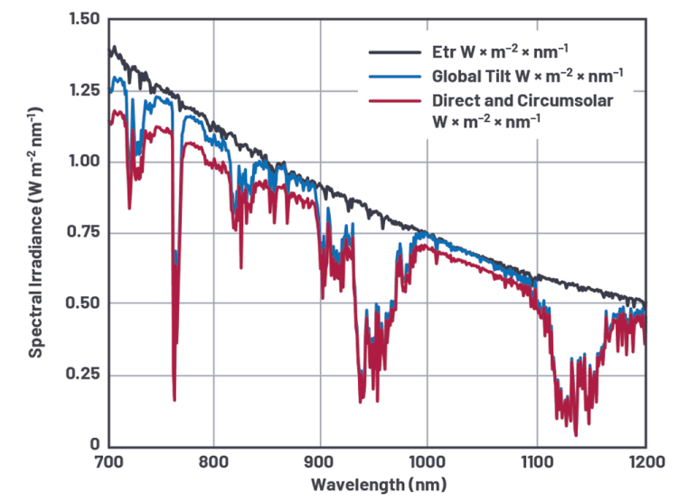
Although the solar emission is maximum in the visible region of the spectrum, the energy in the NIR region is still significant. Sunlight (and ambient light more generally) can increase depth noise and reduce the range of a ToF camera. Fortunately, due to atmospheric absorption, there is a dip in sunlight irradiance in the 920 nm to 960 nm region, where the solar irradiance is less than half that of the 850 nm region (see Figure 3). In outdoor applications, operating the ToF system at 940 nm provides better ambient light immunity and leads to better depth sensing performance.
Radiant intensity (optical power per solid angle)
The light source generates a constant optical power distributed into a 3D space within the FOI produced by the diffusing optics. As the FOI increases, the energy sustained per steradian (sr) – that is, radiant intensity (W/sr) – decreases. It is important to understand the trade-offs between FOI and radiant intensity as they affect the SNR and therefore the depth range, of the ToF system.
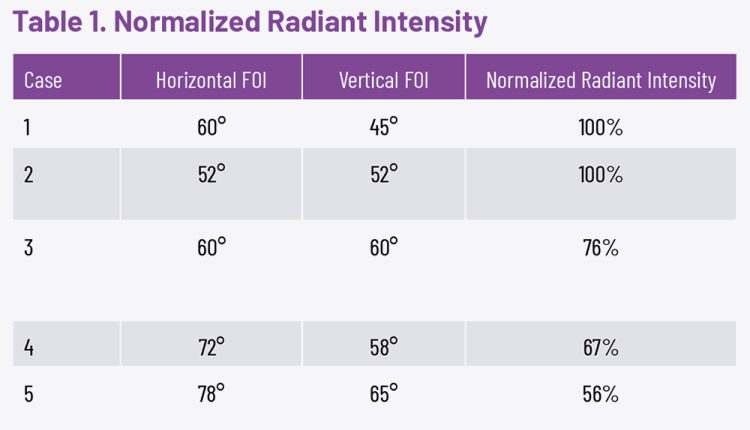
Table 1 lists a few examples of FOI and their corresponding radiant intensity normalised to the radiant intensity of a 60° x 45° FOI. Note that the radiant intensity is calculated as optical power per rectangular solid angle.
Illumination profile specifications
To fully define the illumination profile, several characteristics should be clearly specified, including the profile shape, profile width, optical efficiency (that is, enclosed energy within a certain FOV) and optical power drop-off outside the FOI. The illumination profile specification is normally defined in radiant intensity in angular space. Mathematically it is expressed as:
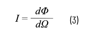
where dΦ is the power emitted into the solid angle dΩ. The FOI needs to match the aspect ratio of the imager and hence is normally square or rectangular.
Illumination profile shape inside FOI
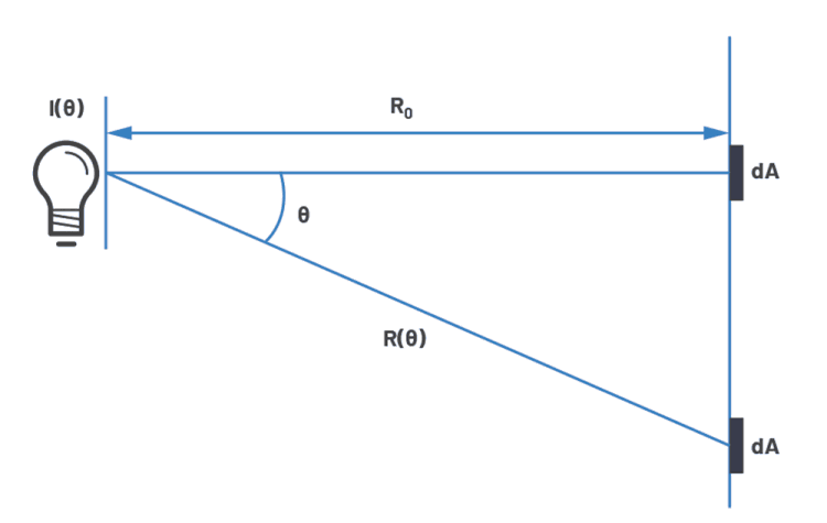
The most common radiant intensity profiles in ToF flood illumination have a batwing shape. They have a profile that varies in cos-n(θ) to compensate for the drop-off (that is, relative illumination) of the imaging lens. Figure 5, demonstrates an example of a batwing illumination profile. If one wishes to achieve constant irradiance on the pixel array of the imager from a flat target, one should also consider a cos3(θ) drop-off factor in irradiance (E) between the target centre and the target edge [W/m2], which is defined as:

where E is irradiance, dA is the surface area illuminated by optical power dΦ, R(θ) is the distance between the light source and dA defined in Figure 4 and dΩ = dA•cos(θ)/R(θ)2.
Width of the profile
The width of the profile determines the FOI of the illumination profile. It can be defined as full-width half-max or 1/e2 of the maximum intensity. To accommodate misalignment between the imaging lens to the imager and the tolerance of the diffuser, FOI is normally designed to be slightly larger than the FOV of the lens to avoid dark pixels.
The width of the profile is the convolution of the intensity profile of the light source to the diffuser response to a collimated beam. The wider the input divergence angle to the diffuser, the wider the width and slower the transition slope. A wider and slower transition slope results in more energy falling outside the FOI, which causes optical power loss. The acceptance criteria for such loss can be specified using the following two requirements.
Optical efficiency – enclosed energy within the imaging lens FOV
This specification defines how much energy will be received by the imaging module and is specified by:

Figure 5c illustrates the concept of 2D integration of the illumination profile within the FOV.
Optical power drop-off outside FOI

In general, the optical efficiency can be improved by having a collimator lens between the light source and the diffuser to reduce the input angle to the diffuser, or by choosing a light source with a smaller divergence angle.
Imaging module
The imaging module consists of an imaging lens assembly, band-pass filter (BPF) and microlens array on the imager. The thickness and material of the backside optical stacks on the imager should be optimised for low back-reflectio. Figure 6 shows an illustration of the imaging module.

ToF imaging lens design considerations
Since the ToF camera collects light generated by active illumination, the efficiency and uniformity of the light collection on the pixel array greatly affect the overall performance. The lens needs to have a strong collecting power, high transmission and low stray light. The following are design considerations for ToF lenses, which are distinct from traditional RGB camera lenses.
Light collecting efficiency
Light collection efficiency is proportional to 1/(f/#)2, where f/# = (focal length)/(aperture size). The smaller the f/#, the better the efficiency. There are some trade-offs with a small f/# optical system. As the aperture size increases, there tend to be more vignetting and aberrations, which make the optics more challenging to design. A low f/# system also tends to have shallower depth of field.
Relative illumination (RI) and chief ray angle (CRA)
RI is defined as:

The sensor illuminance declines based on the (cos q)4 law in a distortion- and vignetting-free lens system, where q is the CRA incident angle on the sensor plane. The result is a relative darkening of the image toward the sensor border. The irradiance fall-off can be reduced by introducing negative distortion in the lens system.
The maximum CRA at the sensor edge should be optimised based on the imager microlens array specification. A smaller CRA helps narrow the bandwidth of the BPF to achieve better ambient light immunity.

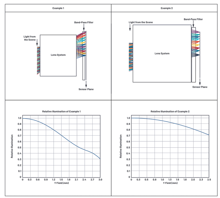
The following examples demonstrate how the CRA and the focused light cone sizes (effective f/#) across the field affect the RI. The lens system of Example 1 in Figure 7 has larger CRAs and gradually decreasing imaging cones (that is, increased f/#) as the field angle increases. The corresponding RI drops significantly with the field angle as shown in the corresponding RI plot. Example 2 in Figure 7 demonstrates that the RI can be well maintained by minimising the CRA as well as keeping uniform f/# across the field.
Stray light
Stray light is any unintended light in a system that could be detected by the sensor. Stray light can come from inside or outside of field sources that form a ghost image (for example, lens flare) through even numbers of reflections. Stray light can also emanate from opto-mechanical structures and any scattering surfaces. ToF systems are particularly sensitive to stray light because the multipath nature of stray light contributes different optical path lengths to a pixel, which leads to depth measurement inaccuracies.
Several strategies in the design process need to be used to reduce stray light, such as optimisation of the anti-reflection (AR) coating and the mechanical aperture, darkening the lens edges and mounting structures and custom design of the BPF to optimise for wavelength and CRA.
The following are some items that can impact stray light in a system:
• Vignetting – Ideally there should not be any vignetting in a ToF lens system. Vignetting cuts off the imaging rays and is sometimes used as a technique to increase the image quality while trading off the brightness of the peripheral fields. However, the cut-off rays often bounce inside the lens system and tend to cause stray light issues.
• AR coating – AR coating on the optical elements reduces the reflectance of each surface and can effectively reduce the impact of lens reflections on depth calculation. AR coatings should be carefully designed for the light source wavelength range and the angle range for the incident angles on the lens surfaces.
• Number of lens elements – Although adding more lens elements provides more freedom to achieve the design specifications and better image quality in terms of resolution, it also increases the inevitable back-reflections from the lens elements as well as increasing complexity and cost.
• Band-pass filter (BPF) – The BPF cuts off ambient light contribution and is essential for ToF systems. The BPF design should be tailored to the following parameters to have the best performance:
(a) Lens parameters such as f/# and CRA across the field.
(b) Light source parameters such as band width, nominal wavelength tolerance and thermal shift.
(c) Substrate material properties to low incident angle drift vs. wavelength or low thermal drift vs. wavelength.
Microlens array
A ToF backside illuminated (BSI) sensor normally has a layer of microlens array that converges rays incident to the image sensor and maximises the number of photons that reach the pixel modulation region. The geometry of the microlens is optimised to achieve the highest absorption within the pixel region where photons are converted into electrons.
In many lens designs, the CRA of the lens increases as the image height increases toward the edge of the sensor, as shown in Figure 8. This oblique incidence leads to absorption loss in the pixel and crosstalk between adjacent pixels when the CRA is too big. It is important to design or choose an imaging lens such that the CRA of the lens matches the specifications of the microlens array it is designed for. For example, the optimal CRA that matches with Analog Devices’ ADSD3100 ToF sensor is around 12° at the sensor horizontal and vertical edges.

Conclusion
ToF optics have unique requirements to achieve optimal performance. This article provides an overview of a 3D ToF camera optical architecture and design guidelines for the illumination and imaging sub-modules to help design such optical systems and/or choose sub-components. For the illumination sub-module, the key factors are power efficiency, reliability and the ability of the light source to be driven at high modulation frequency with high modulation contrast.
Wavelength selection consideration between 850 nm and 940 nm, as well as how to specify the illumination profiles, are discussed in detail. For the imaging sub-module, the lens design considerations including f/#, CRA that matches with the microlens specification and stray light control are critical to system-level performance.
| Tel: | +27 11 923 9600 |
| Email: | [email protected] |
| www: | www.altronarrow.com |
| Articles: | More information and articles about Altron Arrow |
© Technews Publishing (Pty) Ltd | All Rights Reserved