


Smaller, smarter and more powerful are market trends for low-power switched-mode power supply (SMPS) applications.
Smaller requires the SMPS to have a more compact form factor, and thus higher power density. Smarter requires intelligent system-to-system/system-to-human communication to ensure the systems are environment- and human-friendly. More powerful requires the SMPS to output more power to supply energy to many different devices in order to save cost for consumers.
These trends expose engineers to new SMPS design challenges. Because of higher output powers and smaller form factors leading to higher power densities, engineers need to spend more effort improving efficiency and managing overall system heat. At the same time, longer product lifetimes require engineers to optimise SMPS designs at a system level to improve reliability.
Benefits due to these market trends are obvious. A smaller size leads to space saving and makes systems more portable. Energy saving due to higher efficiency and smarter design helps consumers save money on electricity bills, as well as supporting a ‘greener’ world – as less power supplies are needed at home thus there is less pollution in production and less waste when it comes to end-of-life disposal.
Adaptors and chargers, LED lighting, audio SMPS, auxiliary power and industrial power are typical low-power SMPS markets where flyback topology is the most common topology. High-voltage (HV) MOSFETs play a fundamental role in this topology, which means that finding the right MOSFET is critical to meeting the challenges posed by market requirements.
Factors to consider when choosing HV MOSFETs for flyback based application
Determining the ‘right’ MOSFET for a flyback topology requires a solid, system-level understanding as well as the way the MOSFET is used in the application. State-of-the-art flyback designs switch HV MOSFETs at 40 kHz – 100 kHz to reduce the need for EMC optimisation, while other designs switch at higher frequencies in order to achieve size reductions associated with smaller magnetic components. Better light-load efficiency requires lower switching losses and high full-load efficiency requires lower low conduction losses.
For switching losses, Qg and Eoss are important MOSFET device parameters. Qg is closely linked with the effort to drive MOSFETs and smaller values lead to lower driving losses. Eoss is the energy consumed by the MOSFET when it switches on. RDS(on) is an important device parameter and determines conduction losses, which plays a critical role at full-load condition.
MOSFET ESD ruggedness is one area that is gaining more and more attention when it comes to MOSFET selection, as it helps to improve production yield and reduce field returns. Robustness, ease of driving and design-in also have to be considered by engineers who are under pressure to deliver fast time-to-market. VGS(th) and its deviation needs to be considered here: lower VGS(th) makes MOSFETs easier to drive while a smaller VGS(th) deviation gives designers more freedom in SMPS design.
CoolMOS P7 drives higher efficiency and thermal performance
The latest 800 V CoolMOS P7 from Infineon sets a new benchmark in 800 V superjunction technologies and combines best-in-class performance with state-of-the-art ease of use.
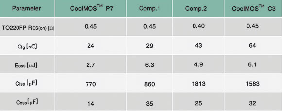
Table 1 gives an overview of key parameters for TO-220 FullPAK products with a maximum RDS(on) rating of between 400 mΩ and 450 mΩ. CoolMOS P7 has been fully optimised to deliver best-in-class performance. Compared to the nearest competitors, Qg and Ciss for CoolMOS P7 is improved by 17% and 10% respectively. In the case of EMoss and Ciss, a dramatic improvement of 43% to 45% has been observed. These optimisations significantly improve CoolMOS P7 efficiency and thermal performance as demonstrated in an 80 W dual stage flyback LED driver application (see Figure 1).
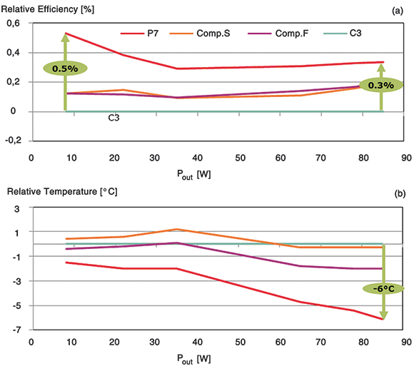
Simply replacing a CoolMOS C3 with a CoolMOS P7 leads to a better efficiency of 0,5% at light-load and an efficiency improvement of 0,3% at full-load condition (see Figure 1 (a)). The improvement at light-load reduces system idle losses, while at full-load the observed efficiency improvement leads to a better MOSFET temperature by 6°C, thus significantly reducing the overhead for thermal management.
There are typically two ways to realise the high power densities required in today’s market. One way is to use a HV MOSFET at high switching frequencies. This delivers better efficiency, while the high-frequency switching enables the system to use smaller magnetic components to reduce system size. CoolMOS P7 is able to address such designs with significantly lower switching losses.
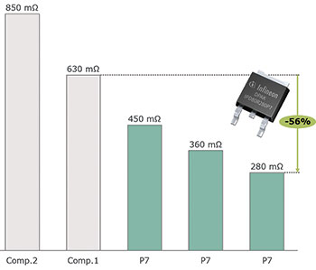
The other method is to use a HV MOSFET with a smaller footprint. CoolMOS P7 also supports this approach by offering DPAK products with lower RDS(on) ratings. As indicated by Figure 2, CoolMOS P7 offers lower DPAK RDS(on) ratings of 450 mΩ, 360 mΩ and 280 mΩ with 280 mΩ as best-in-class, which is 56% lower as than that of the nearest competitors. Better DPAK products help customers save space to increase power density and reduce production costs by utilising fully automatic assembly processes (when changing from through-hole to SMD packages).
One of the most important features for the CoolMOS P7 product family is its integrated Zener diode, which reduces ESD related failures to improve quality and reliability. The Zener Diode is integrated into CoolMOS P7 between the gate and the source (see Figure 3 (a)), where its function is to provide ESD protection. As shown in Figure 3 (b), during an ESD event the voltage between gate and source (VGS) is clamped by the Zener diode.
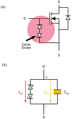
Using the HBM ESD model, CoolMOS P7 ESD ruggedness is Class 1C for RDS(on) values between 2 Ω and 4,5 Ω. Below 2 Ω the HBM ESD ruggedness is Class 2. Using the CDM model, ESD ruggedness is Class C3. This ESD protection feature helps reduce ESD related failures during assembly, leading to lower production costs. It also helps reduce field returns by avoiding gate oxide overstress. This is an issue that leads to reduced MOSFET lifetime, making it possible for a MOSFET that does not fail during assembly to fail in the field.
CooMOSTM P7 offers 12 RDS(on) classes in six package variants for five main target applications: adaptor and charger, LED driver, audio SMPS, auxiliary and industrial power supplies. With fine granularity in RDS(on), designers can easily find a part for fine tuning their designs.
Designing with CoolMOS P7
CoolMOS P7 combines best-in-class efficiency with state-of-the-art ease of use. This product family is ideal for flyback applications with outputs up to 250 W. Infineon supports the design-in of CoolMOS P7 with a variety of application notes and reference designs, including a 45 W adaptor demonstration board.
For more information contact Davis Moodley, Infineon Technologies, +27 (0)11 706 6099, [email protected], www.infineon.com


© Technews Publishing (Pty) Ltd | All Rights Reserved
 printer friendly version