


Silicon carbide (SiC) has advantages over silicon (Si) that make it particularly suitable for Schottky diodes in applications such as fast battery chargers, photovoltaic (PV) battery converters, and traction inverters. Still, designers are being pushed to improve efficiency further.
Two ways to do this with SiC devices are to reduce leakage current and losses due to thermal resistance. While achieving these goals has been challenging, merged-pin Schottky (MPS) diodes offer a solution. MPS devices also enhance Schottky diode surge current performance.
The advantages of SiC Schottky diodes
The advantage of the SiC Schottky diode over a traditional Si P-N junction derives from the properties of the underlying semiconductor material and its design. SiC has a wider bandgap than Si. The bandgap is the energy needed to move electrons from the valence band to the conduction band in a semiconductor, and it is a crucial factor in determining the material’s electrical conductivity.
SiC’s wider bandgap endows it with an order of magnitude higher dielectric breakdown field strength, with a thinner drift layer for the same voltage rating, when compared to an Si device. The drift layer is the lightly doped layer between a conventional diode’s P and N layers, or the metal and P layers of a SiC Schottky diode. The thinner drift layer features lower resistivity and better electrical conduction performance from a smaller die size.
Another benefit of SiC is its approximately 3,5 x better thermal conductivity, which improves power dissipation for a given chip area. The maximum operating temperature of SiC is nearly double that of Si. Utilising a smaller die size decreases device self-capacitance, and the associated charges are lower for a specified current and voltage rating. These characteristics and SiC’s higher electron saturation velocity enable faster switching speeds with reduced losses.
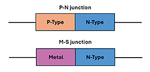
From a construction perspective, instead of the conventional P-N junction, the Schottky diode dispenses with the P-type and instead uses a thin layer of metal (platinum, tungsten, gold, or another metal) bonded to N-type material. This bonding forms a metal-semiconductor (M-S) junction called a Schottky barrier (see diagram).
The M-S junction generates a narrower electron depletion region in forward and reverse bias conditions than the P-N junction. The narrower depletion zone gives the Schottky diode a key advantage: a lower forward voltage (VF) than a conventional diode. When forward biased, the Schottky diode will typically start conduction at a few hundred millivolts compared with 0,6 to 0,7 volts for a P-N junction. This characteristic is advantageous for low-power applications such as battery-powered devices.
Schottky devices conduct only through majority carriers (electrons), which results in negligible charge stored in the diode’s junction depletion layer when the component is forward biased. This limits losses (and power dissipation) when the diode switches from forward to reverse bias. In contrast, P-N junction diodes conduct through minority and majority carriers, which results in greater stored charges in the depletion layer. The outcome is higher switching losses for the P-N device, which multiply with increased frequency.
Overall, a Schottky diode will consume less power and tend to be more thermally efficient at dissipating heat in high-power applications than a P-N device. The reduction in dissipation enables the Schottky diode to withstand higher temperatures for more rugged performance and better reliability without the risk of thermal runaway.
A further advantage of the Schottky diode’s narrow depletion zone is that it endows the component with lower capacitance. Together with the SiC diode‘s soft switching’ behaviour, this low capacitance significantly reduces electromagnetic interference.
SiC Schottky diodes continue to improve. For example, the narrow depletion zone of a contemporary SiC device multiplies the impact of the imperfections that occur when manufacturing the M-S interface, causing high leakage currents when the diode is reverse-biased. Moreover, the narrow depletion zone prevents the SiC Schottky diode from withstanding high reverse voltages (VR). A Schottky diode can withstand a VR of tens of volts, whereas a P-N junction can withstand hundreds of volts.
One solution to address the SiC diode’s high leakage currents is to thicken the diode’s drift layer and substrate. However, this increases electrical and thermal resistance, pushing up VF and junction temperature (TJ) for a given current. Moreover, the thickened drift layer’s higher resistance can impact surge current performance.
Nexperia has addressed this challenge with its MPS diode. The PSC Series’ MPS structure uses two diode types, a SiC Schottky and a P-N device positioned in parallel. P-doped ‘wells’ are implanted in the drift zone of a conventional Schottky device, forming a P-ohmic contact with the metal at the Schottky anode and a P-N junction with the lightly-doped SiC drift.
Under reverse bias, the P-doped wells encourage the maximum field strength to move downwards into the almost defect-free drift layer, away from the metal barrier with its imperfections, reducing the overall leakage current. The result is that an MPS device can operate at a higher breakdown voltage than a conventional SiC diode, but with the same leakage current and drift layer thickness.
| Tel: | +27 11 608 0144 |
| Email: | [email protected] |
| www: | www.nuvisionelec.com |
| Articles: | More information and articles about NuVision Electronics |


© Technews Publishing (Pty) Ltd | All Rights Reserved
 printer friendly version