


This article discusses how the performance of high-speed pipeline analog-to-digital converters (ADC) can be optimised by designing the right clock circuitry, a good analog input network, as well as how to get the data at these high speeds undistorted from the ADC onto an FPGA or ASIC.
With the performance of these ADCs reaching new heights, resolution, sampling speed and dynamic performance are being pushed to new limits. The challenge is to keep the static and especially dynamic performance at the levels that are given in the device-
specific data sheet. Designers must select components around the converter very carefully.
As an example, this article will consider TI’s ADC14V155 which is amongst the best-in-class converters, with a resolution of 14 bits and sampling at up to
155 MSps. See the sidebar for the headline performance figures of this chip.
Clock jitter – the enemy of SNR performance
At high input frequencies and resolution, clock jitter/data jitter becomes one of the biggest limitations to ADC signal-to-noise ratio (SNR) performance. The maximum jitter without degrading SNR must be below the quantisation noise (1/2 LSB) and can be calculated as:
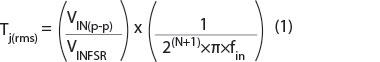
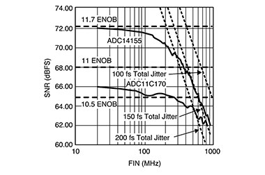
When the input voltage swing VIN(p-p) is optimised to swing full scale the first term becomes one and jitter is only dependent on resolution (N) and input frequency (fin). Measurements of SNR performance on ADCs with 11- to 14-bit resolution shows that for input frequencies above 100 MHz the total system jitter should be no more than 200 fs for the 11-bit ADC and around 100 fs for the ADC14V155 (11,5 ENOB).
Using that information can help target what clock source specification and design to implement. Most clock products are defined by their frequency and phase noise, found in the device-specific data sheet plots. Phase noise and jitter are describing the same phenomenon or problem where phase noise is represented in the frequency domain and jitter is derived from it by integrating the phase noise plot.
Consequently, it provides a good insight on what causes jitter on the ADC clock, which can then be addressed and eliminated by subsequent circuit design. A good start is to divide the diagram into the two areas of close-in phase noise and broadband noise.
Broadband noise can easily be filtered out, so we have to concentrate on the close-in phase noise. A clock source is needed which has low close-in noise and it should roll off as steeply as possible at the lowest offset.
The reason why broadband noise has to be filtered out is that the signal on the ADC clock input is convolved with the analog input. The very high input bandwidth of 1,1 GHz of the ADC14V155 is matched with a very high clock input bandwidth. That means that a lot of the broadband noise from the clock source, if not filtered away, will alias back into the first Nyquist zone and may degrade SNR.
Subsampling pitfalls
If subsampling is used, it is possible to become victim to another trap. Subsampling refers to the situation where the clock frequency is more than twice the signal frequency, which violates the Nyquist theorem which states that fs should be greater than two times fin to avoid aliasing.
Subsampling causes the signal and its harmonics to alias back into the first Nyquist band, but as long as one knows which frequencies they are aliased to, a frequency plan can be laid out in a way such that the signal of interest is not corrupted by aliased harmonic spurs.
One popular frequency plan is to use an input frequency that aliases to fs/4. In this frequency plan, all of the harmonics will alias to DC, fs/4 or fs/2. The benefit of this plan is that it gives the biggest separation between harmonic distortion spurs, which simplifies filtering and centres the fundamental frequency in the Nyquist band.
However, this frequency plan also masks all of the ADC’s harmonic spurs by overlapping them and makes the ADC output spectrum look much better than it actually is. To see the true performance, it is required to offset the input frequency by 0,1 to 1 MHz, which unmasks overlapping spurs.
ADC clock receiver
Unfortunately, even the clock receiver circuitry inside the ADC itself will generate some jitter. The reason for this is that any supply noise will change the clock receiver’s tripping point slightly and this noise will be converted into phase noise when a clock signal with finite slope is applied.
This is an analogy of amplitude modulation (AM) to phase modulation (PM), where AM is the supply noise converted to PM clock noise, which is then jitter in the time domain view. The longer the transition time of the clock, the more jitter is added. Applying a high slew rate clock will minimise this effect. Consequently, a square wave clock input with fast transition times is the best choice and gives the best SNR.
In the lab and for testing concepts, high-quality signal generators are the best option offering frequency agility. Once the frequency plan is fixed, a crystal oscillator provides the purest clock. If multiple clocks are required on the PCB, then one of the LMK03000/2000 series precision clock conditioners from Texas Instruments is a good choice.
The input network
In the selection and testing phase of an ADC, signal generators are used to drive the input. Clearly, the measured ADC performance is no better than the purity of the signal applied to its inputs. That means filtering of the signal generator output is mandatory to limit the generator’s harmonic distortion and noise from reaching the ADC inputs.
A typical synthesiser’s second harmonic distortion (H2) will be between -40 dBc and -50 dBc while the ADC14V155 H2 at 238 MHz can be as low as -85 dBFS. It is recommended to use tuneable bandpass filters like Trilithic VF series filters providing 90 dB 2nd and 3rd harmonic attenuation.
Filtering the input signal is certainly critical in the final product application. The ADC14V155 has an extremely wide input bandwidth of 1,1 GHz, which means it will sample the entire spectrum including all unwanted noise components as described in the sampling pitfalls section.
Even if the ADC samples at only 155 MHz, noise above this frequency will be aliased back into the first Nyquist band, which has a negative effect on SNR, but by bandpass filtering the input signal around its centre frequency, the problem can be avoided.
In most practical examples, the ADC will be coupled to the input signal via a transformer and/or amplifier. Figure 3 shows a circuit example to drive the ADC14V155 using a DVGA LMH6515.
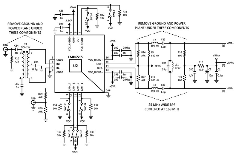
Between the ADC and the amplifier, a fourth order filter with 25 MHz bandwidth centred around 169 MHz is used. The resistors R16 and R19 provide input common mode bias to the ADC and set the load impedance of the filter. Having too high an impedance should be avoided since, although that reduces the filter attenuation, it also degrades SFDR. The best trade-off between ADC and amplifier distortion has been found to be 500 Ω.
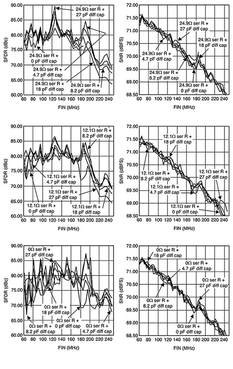
To maximise SFDR performance, an additional RC network can be used and tuned to the application’s input frequency. The network consists of two serial resistors connected to the input pins of the ADC and a shunt capacitor. These resistors and the capacitor affect settling time due to disturbances from the sample-and-hold circuitry at the ADC input.
The RC combination also provides a last lowpass filter before the ADC and the cutoff frequency will impact noise rejection and harmonic attenuation. A higher value shunt capacitor will lower the cutoff frequency of the lowpass filter and will improve low frequency distortion (at the expense of input bandwidth).
Figure 4 shows various frequency sweeps illustrating SFDR performance with different filter settings. The device-specific data sheet of the ADC14V155 shows 12,1 Ω resistors and a 15 pF capacitor, which exhibits a good compromise over a wide fin range.
Decoupling
After selecting the right low-jitter clock and providing a clean, filtered signal to the input of the ADC, there is one more area of focus. Noise can also couple into the ADC through its reference and supply pins. The best practice is to place decoupling capacitors as close as possible to the ADC package and pins.
At least two different capacitor values for decoupling must be used – 0,1 µF and 0,01 µF – and they have to be connected to the power and ground planes directly. Long traces introduce parasitic resistance and inductance, and must be avoided.
While measuring SNR and SFDR performance of the ADC14155 in both LLP and TQFP packages, lead length can be problematic if not addressed. Testing has showed that with the leads length of the TQFP package, the decoupling caps must be placed on the back of the board directly under the reference and supply pin for optimal performance. SNR degraded almost 3 dB with top side decoupling and SFDR degraded over 3 dB.
Output interface
Once the analog signal has been converted, the result can be presented to a further processing step such as an FPGA or ASIC. For many years, CMOS output stages were used to transfer digitised data. The output level of a CMOS stage is load dependent and the signal is voltage mode. A single-ended type output also means no common-mode rejection of noise.
With rising switching speeds, the current to drive capacitive loads increases, reducing CMOS voltage swing. At around 150 MHz the data transfer on a CMOS interface becomes unreliable. A new type of interface has to be used and LVDS is an excellent candidate.
An LVDS driver provides a constant current of 3,5 mA in a differential scheme. 100 Ω termination resistors have to be used between the differential output lines as close as possible to the receiver pins.
The ADC14V155 uses an interleaved DDR output scheme where odd bits are presented first and then even bits on the same pins. The outputs change state at rising and falling clock edges. This saves 50% or 14 pins on the package and the same amount of connections on the receiving device. Besides the data pins, the Over-Range Indicator (OVR) and Data-Ready Strobe (DRDY) are provided in LVDS format.
The ADC14V155 at a glance
The ADC14V155 uses differential pipeline architecture and its unique low jitter sample-and-hold stage yields a full power bandwidth of 1,1 GHz. This high input bandwidth makes it a very good candidate for all types of communication receivers, but especially for undersampling.
The device can sample signals up to 450 MHz bandwidth, providing flexibility for the system frequency planning and allowing migration from single carrier architectures to a multi-carrier approach where a single ADC digitises several carriers.
Another area where this ADC can be used is for fast test and measurement equipment. Data leaves the chip on a parallel low voltage differential signalling (LVDS) interface in a dual data rate (DDR) format to allow clean data transmission onto modern FPGAs.
To further reduce noise and power, the device features a separate power supply for the output interface (1,8 V) and the analog section (3,3 V). Typically the device uses under one Watt power. At input frequencies of 70 MHz, it typically performs with an SNR of 71,7 dBFS and spurious free dynamic range (SFDR) of 86,9 dBFS.
For more information contact Erich Nast, Avnet Kopp, +27 (0)11 319 8600, [email protected], www.avnet.co.za.


© Technews Publishing (Pty) Ltd | All Rights Reserved
 printer friendly version