The first considerations in choosing a voltage reference are output voltage and initial accuracy. Often overlooked, however, are the various other datasheet parameters that can assume major importance in specific applications.
Also, one should be sure to take into account the error budget when evaluating a data converter (ADC or DAC) together with a voltage reference.
The following discussion of voltage reference basics will help readers better understand the common types of voltage references and the performance parameters associated with the most common voltage reference topologies: the two-terminal shunt and the three-terminal series designs.
Common types of voltage references
There are three common types of voltage references: charged capacitor, zener and bandgap. The charged capacitor is little used (particularly in safety applications) because of instability caused by ionising radiation. Alpha, beta, gamma and cosmic rays or common X-rays in airports, hospitals and transport security all discharge the capacitor (typically a 7 mV change to the capacitor at each discharge).
Zeners, the second type of common voltage reference, are used in and out of avalanche mode. Most avalanche mode zeners are used where they would be most stable (i.e., at a sharp knee), above approximately 5,5 V depending on the semiconductor process. True zeners at lower voltages work because of quantum mechanical tunnelling. The majority of zener noise issues are due to associated impurities on the die surface, which are overcome with buried zeners by burying the zener inside or below the die surface.
The most common voltage reference uses a bandgap. This is the clever use of two transistor junctions with different current densities and hence different temperature coefficients. Two voltages with opposing temperature coefficients are subtracted from one another to make a nearly flat temperature curve.
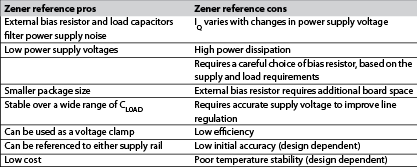
Series and shunt references could use any of the above technologies. The sidebar compares the series and shunt configurations with these various technologies.
Two-terminal shunt reference

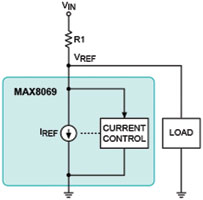
As its name implies, the shunt reference operates in parallel with its load (Figure 1). It can be viewed as a voltage-controlled current sink in which the controlling voltage is applied to its input terminal. With no load applied, the shunt reference sinks just enough current so that the voltage drop across R1 produces the desired output voltage (VIN - IREF·R1 = VREF).
If, for example, VIN = 6,0 V and the desired VREF is 5,0 V, the reference IREF creates a 1,0 V drop across R1. The reference then makes IREF adjustments as necessary to maintain 5,0 V across its input.
Now, if a load is applied to the reference, IREF no longer equals IR1, because load current (IL) produces part of the voltage drop across R1. The reference automatically reduces its sink current by the amount of IL. Thus, the total current through R1 does not change (i.e., IREF + IL equals the original IR1). IR1 is shunted between reference and load, hence the name ‘shunt reference.’ A shunt reference regulates the output voltage by adjusting its sink current to oppose changes in load current.
Three-terminal series reference

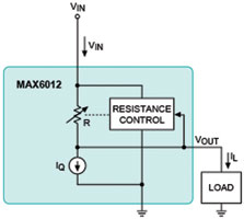
The series reference operates in series with its load (Figure 2). It can be viewed as a voltage-controlled resistance in which VOUT controls an internal resistance between the reference’s input and output terminals.
A series reference regulates by creating a voltage drop between its input and output; the voltage drop is equal to the product of the load current and the controlled internal resistance. With no load applied, the series reference draws a small amount of current (IQ) through the internal resistance (R) to drop a voltage between the input and output necessary to produce the correct VOUT.
As load current increases, the reference maintains the desired output voltage by changing R, as required, to produce the correct drop between input and output. Applying Ohm’s Law, one notes that to maintain a constant drop between input and output, R must decrease as IOUT increases.
Parameter measurement units for references
The units that specify parameters such as accuracy differ among manufacturers. For specifying accuracy, the units in common usage include percentage of full scale (%), parts per million (ppm), decibels (dB) and voltage (V) or microvolts (µV). All are acceptable, but to make ‘apples-to-apples’ comparisons, one must be able to convert one unit to any other unit. These relationships are clarified below.

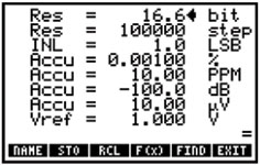
The accuracy calculator in Figure 3 can aid in the design and analysis of voltage references and data converter application circuits. It calculates the DC accuracy of an ideal data converter, covering both analog-to-digital converters (ADCs) and digital-to-analog converters (DACs).
The DC accuracy of a data converter is the measure of the maximum deviation from the ideal linear transfer function. Although the HP handheld calculator is a convenient tool, there is also a free emulator that runs on many computers that use the Windows operating system. For more information on the accuracy calculator, including the free emulator, Google the phrase ‘Steve’s Analog Design Calculators’.
Accuracy percentage of full scale
The most common means for stating reference accuracy is a percent of the nominal value, which is not even a unit. It probably follows the convention for expressing tolerance on resistors, capacitors and inductors. Typical percent accuracy specifications for references are 1%, 1,5%, 2%, 5%, etc. Although percent accuracy is fine for comparing one reference with another, it does not provide specific information about how much the reference voltage fluctuates. What really matters is the variation in volts.
To determine the voltage deviation of a reference specified in percent accuracy, you multiply the reference’s nominal output voltage by the percent accuracy and divide by 100. For example, a 2,5 V reference accurate to ±1,5% has a deviation of:
±(2,5 V X 1,5)/100 = ±0,0375 V, or ±37,5 mV
Because the reference error can be above or below nominal, the total deviation is twice this value, or 75 mV. The total output voltage variation equals the nominal voltage plus or minus the error voltage:
2,5 V ±0,0375 V = 2,4625 V ↔ 2,5375 V
Knowing these voltage limits for the reference provides specific design boundaries for the circuitry supported by the reference.
Accuracy parts per million
Another reference accuracy unit found in data sheets is parts per million, or ppm. This unit is typically used to specify temperature coefficients and other parameters that change very little under varying conditions. For a 2,5 V reference, 1 ppm is one-millionth of 2,5 V, or 2,5 μV. If the reference is accurate to within 10 ppm (extremely good for any reference), its output tolerance is:
2,5 V X 10/10-6 = 25 μV
Converting this to voltage accuracy:
2,5 V ± 25 μV = 2,499975 V ↔ 2,500025 V
Converting to percent:
±(25 X 10-6 V) X 100/2,5 V = ±0,001%
Accuracy in bits
Use of the term ‘bits’ as a unit, as in ‘16-bit reference,’ is somewhat confusing. Does it represent an actual measurement of accuracy, or does it mean that the reference is accurate enough for a 16-bit ADC? A 16-bit reference could be accurate to 1 LSB or 2 LSBs, so it cannot necessarily be considered sufficient for a 16-bit system. However, a reference ‘accurate to 16 bits’ is specified with hard numbers.
If the unit is specified by an actual measurement, then ‘accurate to 16 bits’ is simply the value of the parameter divided by the claimed bit accuracy expressed in decimal form. For example, a 2,5 V reference, claimed to be 16-bit accurate (another extremely accurate tolerance for any reference), should deviate by no more than the decimal equivalent of 16 bits: 216 = 65536. Therefore, 1 bit is 1/65536 of the total value.
In this case, 2,5/65536 ≈ 8 μV. If we assume 1-bit accuracy (±1 LSB), the output voltage can be 1 bit higher or lower than nominal, i.e., ±38 μV.
Converting to voltage accuracy:
2,5 V ±38 μV = 2,499962 V ↔ 2,500038 V
Converting to percent:
(±38 X 10-6 V) X 100 = ±0,0015%
Popular voltage reference types
Two-terminal shunt (zener reference)
A zener reference is based on the zener principle above approximately 5 V, in which the current in a reverse-biased diode begins to flow at a certain voltage threshold and then increases (avalanches) dramatically with an increase in voltage. A resistor in series with the diode establishes a constant current, allowing the zener to achieve a stable reference voltage. The zener reference behaves like a typical shunt or two-terminal reference. It can also be used as a voltage clamp.

Three-terminal series and buried (subsurface) zener references

Two- and three-terminal series (bandgap) references
For applications below approximately 5 V that require a compromise between cost and outstanding performance (low-noise operation and accuracy), the bandgap reference has become one of the most popular voltage references available. It compensates for the effect of temperature by subtracting the negative-tempco voltage of a forward-biased base-emitter junction from a positive-tempco PTAT (proportional to absolute temperature) voltage. The PTAT voltage is generated by measuring and amplifying the voltage difference between two forward-biased diode junctions.

The remainder of this article, which covers important performance parameters, will appear in the next issue of Dataweek.
| Tel: | +27 11 608 0070 |
| Email: | [email protected] |
| www: | www.cstelectronics.co.za |
| Articles: | More information and articles about CST Electronics |

© Technews Publishing (Pty) Ltd | All Rights Reserved