


What is the best way to deal with over-voltage conditions?
The three examples above are the results of analog inputs exceeding a supply – VDD, VSS or GND. Simple protection methods to counter these conditions include the addition of external resistors, Schottky diodes to the supplies, and blocking diodes on the supplies.
Resistors, to limit current, are placed in series with any switch channel that is exposed to external sources (Figure 8). The resistance must be high enough to limit the current to approximately 30 mA (or as specified by the absolute maximum ratings).
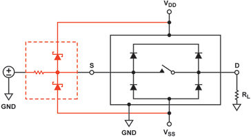
The obvious downside is the increase in RON (ΔRON) per channel, and ultimately the overall system error. Also, for applications using multiplexers, faults on the source of an off channel can appear at the drain, creating errors on other channels.
Schottky diodes connected from the analog inputs to the supplies provide protection, but at the expense of leakage and capacitance. The diodes work by preventing the input signal from exceeding the supply voltage by more than 0,3 V to 0,4 V, ensuring that the internal diodes do not forward-bias and current does not flow.
Diverting the current through the Schottky diodes protects the device, but care must be taken not to overstress the external components.
A third method of protection involves placing blocking diodes in series with the supplies (Figure 9), blocking current flow through the internal diodes. Faults on the inputs cause the supplies to float, and the most positive and negative input signals become the supplies.
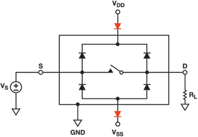
As long as the supplies do not exceed the absolute maximum ratings of the process, the device should tolerate the fault. The downside to this method is the reduced analog signal range due to the diodes on the supplies. Also, signals applied to the inputs may pass through the device and affect downstream circuitry.
While these protection methods have advantages and disadvantages, they all require external components, extra board area and additional cost. This can be especially significant in applications with high channel count.
To eliminate the need for external protection circuitry, designers should look for integrated protection solutions that can tolerate these faults. Analog Devices offers a number of switch/mux families with integrated protection against power-off, over-voltage and negative signals.
What pre-packaged solutions are available?
The ADG4612 and ADG4613 from Analog Devices offer low on-resistance and distortion, making them ideal for data acquisition systems requiring high accuracy. The on-resistance profile is very flat over the full analog input range, ensuring excellent linearity and low distortion.
The ADG4612 family offers power-off protection, over-voltage protection and negative-signal handling, all conditions a standard CMOS switch cannot handle.
When no power supplies are present, the switch remains in the off condition. The switch inputs present a high impedance, limiting current flow that could damage the switch or downstream circuitry.
This is very useful in applications where analog signals may be present at the switch inputs before the power is turned on, or where the user has no control over the power supply sequence. In the off condition, signal levels up to 16 V are blocked. Also, the switch turns off if the analog input signal level exceeds VDD by Vτ.
Figure 10 shows a block diagram of the family’s power-off protection architecture. Switch source and drain inputs are constantly monitored and compared to the supply voltages, VDD and VSS.
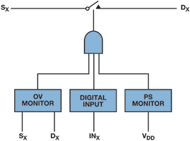
In normal operation the switch behaves as a standard CMOS switch with full rail-to-rail operation. However, during a fault condition where the source or drain input exceeds a supply by a threshold voltage, internal fault circuitry senses the over-voltage condition and puts the switch in isolation mode.
Analog Devices also offers multiplexers and channel protectors that can tolerate over-voltage conditions of +40 V/–25 V beyond the supplies with power (±15 V) applied to the device, and +55 V/–40 V unpowered. These devices are specifically designed to handle faults caused by power-off conditions.
These devices comprise N-channel, P-channel and N-channel MOSFETs in series, as illustrated in Figure 11. When one of the analog inputs or outputs exceeds the power supplies, one of the MOSFETs switches off, the multiplexer input (or output) appears as an open circuit, and the output is clamped to within the supply rail, thereby preventing the over-voltage from damaging any circuitry following the multiplexer.
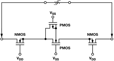
This protects the multiplexer, the circuitry it drives, and the sensors or signal sources that drive the multiplexer. When the power supplies are lost (through, for example, battery disconnection or power failure) or momentarily disconnected (rack system, for example), all transistors are off and the current is limited to subnanoampere levels.
The ADG508F, ADG509F and ADG528F include 8:1 and differential 4:1 multiplexers with such functionality. The ADG465 single- and ADG467 octal-channel protectors have the same protective architecture as these fault-protected multiplexers, without the switch function. When powered, the channel is always in the on condition, but in the event of a fault, the output is clamped to within the supply voltages.
Latch-up
What is a latch-up condition?
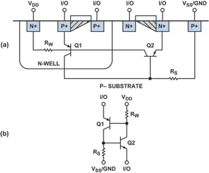
Latch-up may be defined as the creation of a low-impedance path between power supply rails as a result of triggering a parasitic device. Latch-up occurs in CMOS devices: intrinsic parasitic devices form a PNPN SCR structure when one of the two parasitic base-emitter junctions is momentarily forward-biased (Figure 12).
The SCR turns on, causing a continuing short between the supplies. Triggering a latch-up condition is serious: in the ‘best’ case, it leads to device malfunction, with power cycling required to restore the device to normal operation; in the worst case, the device (and possibly power supply) can be destroyed if current flow is not limited.
The fault and over-voltage conditions described earlier are among the common causes of triggering a latch-up condition. If signals on the analog or digital inputs exceed the supplies, a parasitic transistor is turned on.
The collector current of this transistor causes a voltage drop across the base emitter of a second parasitic transistor, which turns the transistor on and results in a self-sustaining path between the supplies. Figure 12(b) clearly shows the SCR circuit structure formed between Q1 and Q2.
Events need not last long to trigger latch-up. Short-lived transients, spikes or ESD events may be enough to cause a device to enter a latch-up state. Latch-up can also occur when the supply voltages are stressed beyond the absolute maximum ratings of the device, causing internal junctions to break down and the SCR to trigger.
The second triggering mechanism occurs if a supply voltage is raised enough to break down an internal junction, injecting current into the SCR.
What is the best way to deal with latch-up conditions?
Protection methods against latch-up include the same protection methods recommended to address over-voltage conditions. Adding current-limiting resistors in the signal path, Schottky diodes to the supplies, and diodes in series with the supplies – as illustrated in Figures 8 and 9 – all help to prevent current from flowing in the parasitic transistors, thereby preventing the SCR from triggering.
Switches with multiple supplies may have additional power supply sequencing issues that may violate the absolute maximum ratings. Improper supply sequencing can lead to internal diodes turning on and triggering latch-up.
External Schottky diodes, connected between supplies, will adequately prevent SCR conduction by ensuring that when multiple supplies are applied to the switch, VDD is always within a diode drop (0,3 V for Schottky) of these supplies, thereby preventing violation of the maximum ratings.
What pre-packaged solutions are available?
As an alternative to using external protection, some ICs are manufactured using a process with an epitaxial layer, which increases the substrate- and N-well resistances in the SCR structure. The higher resistance means that a harsher stress is required to trigger the SCR, resulting in a device that is less susceptible to latch-up.
An example is the Analog Devices iCMOS process, which made possible the ADG121x, ADG141x and ADG161x switch/mux families. For applications requiring a latch-up-proof solution, new trench-isolated switches and multiplexers guarantee latch-up prevention in high-voltage industrial applications operating at up to ±20 V.
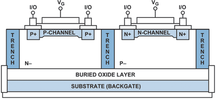
The ADG541x and ADG521x families are designed for instrumentation, automotive, avionics and other harsh environments that are likely to foster latch-up. The process uses an insulating oxide layer (trench) placed between the N-channel and the P-channel transistors of each CMOS switch.
The oxide layers, both horizontal and vertical, produce complete isolation between devices. Parasitic junctions between transistors in junction-isolated switches are eliminated, resulting in a completely latch-up-proof switch.
The industry practice is to classify the susceptibility of inputs and outputs to latch-up in terms of the amount of excess current an I/O pin can source or sink in the over-voltage condition before the internal parasitic resistances develop enough voltage drop to sustain the latch-up condition. A value of 100 mA is generally considered adequate.
Devices in the ADG5412 latch-up proof family were stressed to ±500 mA with a 1 ms pulse without failure. Latch-up testing at Analog Devices is performed according to EIA/JEDEC-78 (IC Latch-Up Test).
ESD - Electrostatic discharge
What is an electrostatic discharge event?
Typically the most common type of voltage transient that a device is exposed to, ESD can be defined as a single, fast, high-current transfer of electrostatic charge between two objects at different electrostatic potentials.
We frequently experience this after walking across an insulating surface such as a rug, storing a charge, and then touching an earthed piece of equipment, resulting in a discharge through the equipment, with high currents flowing in a short space of time.
ICs can be damaged by the high voltages and high peak currents generated by an ESD event. The effects of an ESD event on an analog switch can include reduced reliability over time, the degradation of switch performance, increased channel leakage or complete device failure.
ESD events can occur at any stage of the life of an IC, from manufacturing through testing, handling, OEM user and end user operation. In order to evaluate an IC’s robustness to various ESD events, electrical pulse circuits modelling the following simulated stress environments were identified: human body model (HBM), field-induced charged device model (FICDM) and machine model (MM).
What is the best way to deal with ESD events?
ESD prevention methods, such as maintaining a static-safe work area, are used to avoid any build up during production, assembly and storage. These environments, and the individuals working in them, can generally be carefully controlled, but the environments in which the device later finds itself may be anything but controlled.
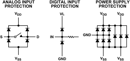
Analog switch ESD protection is generally in the form of diodes from the analog and digital inputs to the supplies, as well as power supply protection in the form of diodes between the supplies, as illustrated in Figure 14.
The protection diodes clamp voltage transients and divert current to the supplies. The downside of these protection devices is that they add capacitance and leakage to the signal path in normal operation, which may be undesirable in some applications.
For applications that require greater protection against ESD events, discrete components such as Zener diodes, metal-oxide varistors (MOVs), transient voltage suppressors (TVS) and diodes are commonly used. However, they can lead to signal integrity issues due to the extra capacitance and leakage on the signal line; this means design engineers need to carefully consider the trade-off between performance and reliability.
What pre-packaged solutions are available?
While the vast majority of Analog Devices switch/mux products meet HBM levels of at least ±2 kV, others go beyond this in robustness, achieving HBM ratings of up to ±8 kV. ADG541x family members have achieved a ±8 kV HBM rating, a ±1,5 kV FICDM rating and a ±400 V MM rating, making them industry leaders, combining high-voltage performance and robustness.
Conclusion
When switch or multiplexer inputs come from remotely located sources, there is an increased likelihood that faults can occur. Over-voltage conditions may occur due to systems with poorly designed power supply sequencing or where hot-plug insertion is a requirement.
In harsh electrical environments, transient voltages due to poor connections or inductive coupling may damage components if not protected. Faults can also occur due to power supply failures where power connections are lost while switch inputs remain exposed to analog signals.
Significant damage may result from these fault conditions, possibly causing damage and requiring expensive repairs. While a number of protective design techniques are used to deal with faults, they add extra cost and board area and often require a trade-off in switch performance; and even with external protection implemented, downstream circuitry is not always protected.
Since analog switches and multiplexers are often a module’s most likely electronic components to be subjected to a fault, it is important to understand how they behave when exposed to conditions that exceed the absolute maximum ratings.
Switch/mux products, like the devices mentioned here, are available with integrated protection, allowing designers to eliminate external protection circuitry, reducing the number and cost of components in board designs. Savings are even more significant in applications with high channel count.
Ultimately, using switches with fault protection, over-voltage protection, immunity to latch-up and a high ESD rating yields a robust product that meets industry regulations and enhances customer and end-user satisfaction.
| Tel: | +27 11 923 9600 |
| Email: | [email protected] |
| www: | www.altronarrow.com |
| Articles: | More information and articles about Altron Arrow |


© Technews Publishing (Pty) Ltd | All Rights Reserved
 printer friendly version