
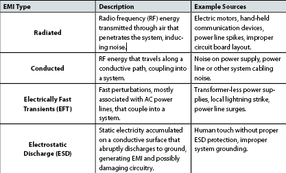
Electromagnetic interference (EMI) is defined as any electromagnetic disturbance that interrupts, obstructs or otherwise degrades or limits the effective performance of electronic equipment. Unfortunately, EMI sources are plentiful and give rise to seemingly endless combinations of disturbance characteristics. For this reason, the industry categorises different types of EMI by their characteristics, as summarised in Table 1.
Medical environments are electrically noisy; RF interference (RFI) generated by communications devices and local equipment can produce RF fields of 50 V/m or more. In addition, certain types of medical equipment use RF energy for diagnosis or treatment (e.g. MRI systems) or wireless communication (e.g. medical telemetry systems).
Given these numerous and potent sources, EMI management in medical environments can be challenging.
EMI impact in medical applications
EMI can cause medical devices to malfunction with potentially catastrophic results. For example, errant signals induced by EMI can cause portable life support systems to malfunction, corrupt measurements in patient monitoring equipment and change patient intravenous medicine dosage levels.
EMI is especially problematic in medical systems that acquire low-amplitude signals, such as electrocardiographs (ECGs), where signals collected from patients can range from 400 μV to 5 mVpk with 3 dB corner frequencies at 0,05 and 100 Hz. Looking forward, the trend towards higher-frequency, lower-power medical systems will complicate EMI management by emitting broader bandwidth RF noise at higher energy levels.
From a design point of view, EMI effects can be minimised by designing system circuitry for high EMI immunity and low emission. Traditional practices include proper printed circuit board (PCB) layout and grounding, and limited trace lengths. Electronic components must be optimally placed on a PCB, and the system enclosure design, cable shielding and filtering must be adequate.
Obviously, the use of EMI-hardened semiconductor components (i.e. low-emission and high-immunity) should be used in critical signal paths. This is especially true for EMI issues that exist within the system itself, such as in mixed-signal or wireless data transmission applications.
Isolation in medical systems
To ensure that medical electronic systems are immune to disturbances from localised fields and other phenomena, isolators are safety tested to a number of IEC-61000 standards using test limits specified by IEC 60601-1-2 as shown in Table 2.
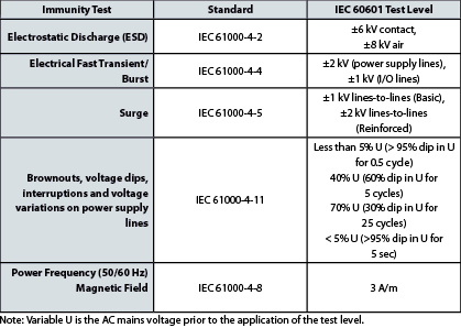
For example, electrostatic discharge (ESD) is tested to IEC 61000-4-2 and uses the test limits specified by IEC 60101-1-2. RF emissions and power line perturbations are tested using methods from CISPR11 test methodology, a subset of automotive specification J1750.
The criteria for passing these tests are very stringent. The system cannot exhibit any component failures, parametric changes, configuration errors or false positives. In addition to external field immunity, the system under test cannot generate significant radiated or conducted emissions of its own.
Specifications published by various agencies place limits on conducted and radiated EMI. One of the more common specifications is FCC Part 15, which covers circuit assemblies used in or near the home. Testing to this specification is conducted in an open-air environment using a 10 metre antenna positioned approximately 5 metres above the ground plane.
Another specification, SAEJ1752-3, is more IC-centric in its test methodology and recommends mounting the IC to be tested on a small shielded circuit board (i.e. ‘TEM cell’, per CISPR11 test methodology) designed to measure only the radiated emissions from the isolator itself while operating within the actual application environment.
EMI hardened silicon isolators
Many medical systems incorporate galvanic isolation to protect patients and equipment from hazardous voltages, to level-shift signals between ground voltage domains and/or to mitigate ground noise in highly sensitive circuit areas.
Medical electronic systems often use transformers and/or optocouplers for signal isolation, neither of which is optimal. Transformers generate EMI and are highly susceptible to signal corruption by external magnetic fields. Optocouplers offer the benefits of low EMI emission and high immunity but suffer from poor reliability and low common-mode transient immunity (CMTI), the latter of which can negatively impact isolator data transmission integrity.
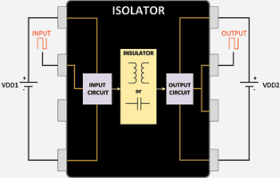
As an alternative to transformers and optocouplers, silicon isolators leverage advanced process technologies to dramatically improve EMI characteristics and create significant gains in performance and reliability. These isolators fabricate insulating devices directly on the semiconductor die using process oxides or other native process materials as shown in Figure 1. The more successful silicon isolator suppliers implement the insulator (aka isolation barrier) using either transformers or capacitors.
The silicon isolator of Figure 2A operates by encoding the logic state of each incoming digital edge, transmitting this data through isolation transformer T1, then decoding and storing the data in an output latch. Figure 2B shows the radiated EMI response from this device, as measured using the CISPR test methodology standards described above.
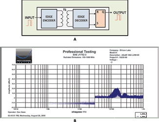
The measurement shown was made with all isolator inputs low and 90 degree rotation. Note that the device generates EMI resonant peaks as high as +20 dB between 100 and 300 MHz. While the exact cause of these resonant peaks is unknown, it is assumed they are at least partially caused by T1’s structural size, inductance and Q.
The silicon isolator in Figure 3A operates by transmitting a carrier wave across the differential capacitive isolation barrier when the isolator input is logic-high. The receiver asserts logic-high on the output when sufficient carrier energy is detected. Unlike the transformer design, there is no Q-dependant resonant peak in the capacitive isolation path to selectively boost incoming EMI frequencies.
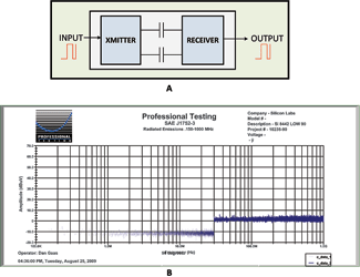
Figure 3B shows the radiated EMI response from this device as measured using exactly the same methodology used in the transformer-based isolator test. This device exhibits a flat, lower-amplitude radiated EMI response compared to the transformer implementation. As a result, this device passed FCC Class B Part 15 in a test using 6-channel differential capacitive isolators with all inputs tied high to maximise internal transmitter emissions.
Figure 4 shows an electric field immunity comparison between the transformer and capacitor-based silicon isolators where isolator output voltage is monitored while the external RF field frequency is swept from DC to 10 GHz. Both the transformer and capacitive isolators have grounded inputs to hold their outputs low continuously.
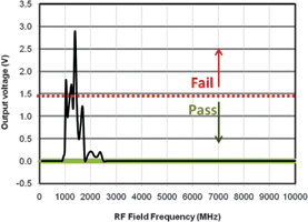
The capacitive silicon isolator output (green trace) remains low across the frequency range from DC to 10 GHz, whereas the transformer-based isolator output is high (corrupted) between 1 and 2 GHz.
The capacitive isolator demonstrates high EMI immunity because local common-mode fields are rejected by a combination of the differential capacitive isolation path and high receiver selectivity. That is, signal levels on each side of the internal differential signal path cause the receiver to amplify only the differential input voltage within a very narrow frequency band but reject all other input.
Figure 5 shows the magnetic field immunity of the transformer and capacitor-based silicon isolators. To meet the requirements of IEC61000-4-9, the isolator must operate normally while subjected to the flux density versus frequency curve shown by the purple line at the bottom of the chart. Values at or above the purple line are acceptable, while values below the line are failures.
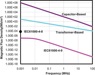
The point placed midway up the Y-axis is the single-point equivalent specification (61000-4-8). Note that both silicon isolators meet the criteria for both specifications, but the capacitive isolator demonstrates a much higher degree of magnetic field immunity compared to the transformer-based isolator.
Summary
EMI can degrade the effective performance of electronic equipment. EMI can cause medical devices to malfunction with potentially catastrophic results including patient trauma or death. Galvanic isolation is required in many medical systems, and it is important that this isolation have a very high EMI immunity and not create EMI emissions of its own. Accordingly, isolators are safety tested to a number of IEC-61000 standards to ensure device safety, low EMI emission and high immunity.
Silicon isolators offer many performance advantages over optocouplers and transformers and typically implement the isolation barrier using chip-scale transformers or capacitors. Transformer-based silicon isolators characteristically have lower EMI immunity and higher emissions compared to capacitor-based silicon isolators. As such, capacitive silicon isolators are ideal for EMI-hardened applications such as medical electronics.
For more information contact Gary de Klerk, NuVision Electronics, +27 (0)11 608 0144, [email protected], www.nuvisionelec.co.za
| Tel: | +27 11 608 0144 |
| Email: | [email protected] |
| www: | www.nuvisionelec.com |
| Articles: | More information and articles about NuVision Electronics |

© Technews Publishing (Pty) Ltd | All Rights Reserved