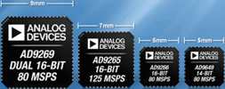

Analog Devices expanded its low-power data converter portfolio with 26 ADCs (analog-to-digital converters) for high-performance, power-efficient communications, portable device, instrumentation and healthcare applications. The three highlights among the new introductions are the AD9269, AD9265 and AD9266.
The dual-channel AD9269 is a 16-bit ADC that consumes 93 mW per channel. It is a monolithic, dual-channel, 20/40/65/80 MSps device, featuring a high-performance sample-and-hold circuit and on-chip voltage reference. The chip includes a QEC (quadrature error correction) and DC offset digital processing block. These blocks dynamically minimise the errors produced in an in-phase/quadrature (I/Q) complex signal receiver system. By using the QEC block, system designers can relax component matching requirements by reducing gain and phase errors due to component mismatches. The net result can also enable a more robust receiver design. In addition, the DC-offset algorithm minimises offsets commonly found in DC-coupled applications.
The AD9269 uses multistage differential pipeline architecture with output error correction logic to provide 16-bit accuracy at 80 MSps data rates and guarantees no missing codes over the full operating temperature range. The ADC operates from a 1,8 V supply and contains several features designed to maximise flexibility and minimise system cost, such as programmable clock and data alignment and programmable digital-test-pattern generation.
The single-channel AD9265, 16-bit ADC was designed to support communications applications requiring low bill-of-material costs, small size and flexibility. Consuming only 370 mW, the ADC core features a multistage, differential pipelined architecture with integrated output error correction logic. The device features a wide bandwidth differential sample-and-hold analog input amplifier supporting a variety of user-selectable input ranges. An integrated voltage reference eases design considerations. A duty cycle stabiliser provides means to compensate for variations in the ADC clock duty cycle, allowing the converters to maintain high performance. The ADC output data are either parallel 1,8 V CMOS or 1,8 V LVDS (DDR). Flexible power-down options allow significant power savings, when desired. Programming for setup and control are accomplished using a 3-bit SPI-compatible serial interface.
The single-channel AD9266 is a 16-bit, low-power ADC available in a small 5 x 5 mm package, with a pin-out that supports resolutions from 10 to 16 bits. The multistage ADC core is based on a proprietary sample-and-hold circuit and on-chip voltage reference. The product uses a differential-pipeline architecture with output-error-correction logic to provide 16-bit accuracy at 80 MSps data rates and guarantees no missing codes over the full operating temperature range. The ADC contains features such as programmable clock and data alignment and programmable digital test pattern generation. The available digital test patterns include built-in deterministic and pseudorandom patterns, along with custom user-defined test patterns entered via the SPI.
The AD9266’s differential clock input controls all internal conversion cycles. An optional DCS compensates for wide variations in the clock duty cycle while maintaining high overall ADC performance. The digital output data are presented in offset binary, Gray code, or two’s complement formats at double-data-rate low
-voltage CMOS levels. A data output clock (DCO) is provided to ensure proper latch timing with receiving logic.

© Technews Publishing (Pty) Ltd | All Rights Reserved