A wide range of timing solutions is available, including crystal oscillators (XO), voltage-controlled crystal oscillators (VCXO) and clocks. A ‘no one size fits all’ strategy applies when it comes to component selection.
Picking the right device for a particular application is dependent on a number of factors, including whether or not the clocks must be synchronised to an externally provided reference clock, the system architecture of the processor and high-speed serial data transmission ICs, and the frequency and jitter requirements of the end application. In high performance applications, low jitter and low phase noise are critical given that they have a direct impact on the bit-error rate in high-speed serial data transmission applications and the signal-to-noise ratio of analog to digital data converters.
Hardware design in high-performance applications such as networking, wireless/RF transmission, broadcast video and test and measurement is becoming increasingly complex as hardware designers grapple with the need to support a growing number of standards, protocols and specifications within a single hardware design. A few examples illustrate this trend.
The latest networking gear is being designed to support not only SONET/SDH and Ethernet, but also high-definition video transmission. Next generation wireless infrastructure equipment is being designed to support both WiMAX and LTE (long-term evolution). Broadcast video equipment, which spans a wide variety of functions including image capture, encoding, decoding, processing and video transport, must support NTSC and PAL standards to ensure worldwide compatibility. As the lines between traditionally different types of equipment become increasingly blurred, a separate challenge arises. Designing the most efficient timing architecture is paramount in these applications to minimise design time and BOM cost.
Asynchronous clocking
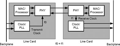
The simplest clock generation source is an oscillator (XO), which generates a single output frequency for a single component. XOs are oftentimes used in asynchronous applications, as shown in Figure 1. Each oscillator provides a local reference to maintain two independent clock domains. System operation requires that XO frequencies be close but not identical. This architecture is ideal for burst-mode traffic applications. Continuous communication requires bit or packet stuffing and FIFO management to prevent overflow/underflow conditions. Video processing equipment and 10/100/1000 Base-T Ethernet are examples of applications that use asynchronous clocking. XO selection should be based on the frequency, jitter and stability requirements of the end application.

Synchronous clocking
Synchronous clocking is most often used in applications that require continuous communication. Network latency and variability in latency must be minimised. To accomplish this, applications including SONET/SDH, Synchronous Ethernet (SyncE), wireless backhaul and video transport require that the source and destination operate at the same frequency.

On the transmit side, the clocks that provide timing for the transmit path of the high-speed SerDes are locked to a highly accurate reference clock. Both primary and secondary reference clocks are supplied from a centralised timing source (eg, GPS). A PLL is used to lock to this backplane reference, attenuate jitter on the clock signal to remove unwanted noise, and provide a low jitter output clock to the PHY.
On the receive side, a clock and data recovery (CDR) unit is used to recover the system clock. This CDR may be an external component or integrated within the PHY, depending on the application. An XO may be used to centre the CDR to provide fast acquisition and lock. The recovered clock passes through another PLL to divide the clock frequency down to a lower rate. Local timing can either be synchronised to this clock or to another local clock that is synchronised to a centralised timing source. Synchronisation to the source ensures clock synchronisation across all nodes in the network. Depending on system requirements, the PLLs used in this application may require a low loop bandwidth to filter unwanted jitter from the clock signal.
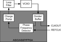
The PLL can be implemented discretely using an integrated clock IC or a voltage-controlled crystal oscillator (VCXO), phase detector and loop filter. A discrete solution is preferable when the lowest possible jitter and best possible phase noise are required. In some applications, processors or ASICs integrate the phase detector and charge pump within the IC so that only a VCXO and external loop filter are required, as shown in Figure 3.

However, there are multiple disadvantages with a discrete PLL solution. A discrete PLL requires analog design expertise and is sensitive to board-level noise, so special care must be taken in the design and PCB layout. In addition, a discrete PLL typically provides a single output frequency. If the design’s frequency requirements change, a separate VCXO must be sourced. In some applications, multiple VCXOs are required to generate all of the required frequencies in the application, increasing BOM complexity. To address these shortcomings, dual, quad and even any-rate I2C-programmable VCXOs like Silicon Labs’ Si571 are available to address multi-rate applications by replacing multiple discrete VCXOs with a single device.
An alternative approach is to use a jitter attenuating clock multiplier IC, which integrates PLL circuitry on-chip. The clock multiplier maintains lock to the reference clock, filters unwanted jitter and generates a multiplied frequency output clock for the transmitter. Special care must be taken in clock multiplier IC selection, as all clock multipliers are not created equal.
For high-speed serial data transmission applications, only the highest performance clock multiplier ICs provide the jitter performance necessary to meet the end application requirements. The key specification is maximum jitter generation as opposed to typical jitter generation. A clock multiplier that specifies maximum jitter best enables the hardware designer to allocate a jitter budget among the data path and timing components in the board and ensure there is sufficient margin under all conditions. Also, the loop bandwidth options available on the clock multiplier IC should be checked. If jitter attenuation of the reference clock is required, then oftentimes the loop bandwidth must be 1 kHz or less. Lastly, the designer must confirm that the clock multiplier IC supports all required frequency plans.
Lastly, a clock solution is preferable to a discrete solution when system-level clock functions are required. An example of this is hitless switching between input clocks, in which the clock monitors the quality of a primary reference clock and switches to a secondary reference upon detection of an alarm condition on the primary clock. Another popular system-level clock requirement is holdover, in which the clock continues to generate a stable output clock in the absence of a valid reference clock.
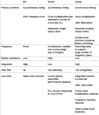
Table 1 summarises when an XO, VCXO or clock solution should be used. Picking the right clock or oscillator for an upcoming design can be greatly simplified by following the guidelines listed above.

For more information contact Gary de Klerk, NuVision Electronics, +27 (0)11 894 8214, [email protected], www.nuvision.co.za
| Tel: | +27 11 608 0144 |
| Email: | [email protected] |
| www: | www.nuvisionelec.com |
| Articles: | More information and articles about NuVision Electronics |

© Technews Publishing (Pty) Ltd | All Rights Reserved