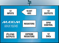

Maxim has introduced the MAX16046-MAX16049, 12-/8-channel, EEPROM-configurable voltage sequencers/monitors/marginers. These devices use unique non-volatile fault registers to store system voltage and fault information upon a critical system failure.
Preserving critical system data in non-volatile memory lets users identify a failing voltage rail and isolate the cause of board failures during test debug or failure analysis.
These devices sequence, reverse sequence, monitor, and margin up to 12 supplies (MAX16046/MAX16047) or eight supplies (MAX16048/MAX16049). Principal applications are high-reliability systems such as storage, telecom and networking equipment where a large number of voltage rails exist in a single system.
Traditional system-monitoring systems: costly and convoluted
Historically, the more complex the application, the more convoluted the monitoring system required. Designers typically use several discrete devices to monitor on-board system conditions. These devices are numerous and spread across the board, which consumes valuable board space. Additional hardware is needed for timeout delays and programming. All this leads to higher costs and longer development time.
The MAX16046-MAX16049 greatly simplify this system-monitoring function. A high-performance ADC eliminates the need for discrete comparators; the internal, 1% accurate ADC measures each input voltage and compares the result to one upper, one lower, and one selectable upper or lower threshold limit. Users benefit because this precision and high speed provides a faster response time. Users would have typically needed 36 external comparators to monitor two undervoltage and one overvoltage thresholds for a 12-channel system.
Identify premature failures, help reduce manufacturing costs
Margining system voltages is an effective means of stress-testing high-reliability systems. This feature is especially important for applications where field failures are unacceptable. With these devices, manufacturers can identify premature failures during the manufacturing process, so their customers are not disrupted and costly returns are avoided.
The 12/8 DAC outputs of the MAX16046/MAX16048 devices are under I²C or logic input control and make it easy to implement power-supply voltage margining during the development phase, qualification phase, and production test. The DAC outputs are connected to the feedback node or trim input of the power supplies. A margining calculator is included in the configuration GUI program to facilitate resistor and DAC value calculations.
Simplify power-up and power-down
Highly complex system controllers require precise power-up and power-down voltage sequencing. Traditionally, board layouts were fixed and these layouts were time-consuming and expensive to change. In addition, it was notoriously difficult, if not impossible, to both sequence and reverse-sequence power supplies with the same topology. Customers can avoid these problems with the MAX16046-MAX16049, because the new devices dynamically sequence up and reverse sequence in any order.
The devices also have integrated charge pumps and a voltage ramp generator that can be used to track up to four system voltages in a closed-loop system. The devices charge the gate of a series-pass nMOSFET with a controlled ramp rate to power up the system voltages, all tracking within 250 mV. Users will benefit because they can now control power-up and power-down for mixed-mode (sequencing/tracking) systems.
Multiple communication interfaces extend application options
Internal EEPROM stores the chip configuration. The configuration is copied to working registers on power-up. The devices are also configurable on-the-fly through the I²C-/SMBus-compliant or JTAG standard interfaces. The EEPROM is in-circuit programmable over both the JTAG and I²C interfaces.
Designed for compact architectures
Multipurpose GPIOs are another desirable feature of the MAX16046-MAX16049. These GPIOs are EEPROM-configurable as dedicated fault outputs, a watchdog input or output, a manual reset, or as margin-control inputs. These flexible GPIOs save pin count, another means of reducing board space.
The devices have a wide 3 V to 14 V operating voltage range. They can be powered directly from a 12 V intermediate bus, thus reducing the number of external components required. They are fully specified over the -40 to +85°C temperature range and are offered in a 56-pin, 8 mm x 8 mm TQFN package.
For more information contact CST Electronics, +27 (0)11 608 0070, [email protected], www.cstelectronics.co.za
| Tel: | +27 11 608 0070 |
| Email: | [email protected] |
| www: | www.cstelectronics.co.za |
| Articles: | More information and articles about CST Electronics |
© Technews Publishing (Pty) Ltd | All Rights Reserved