


This article describes the design of negative-resistance oscillators by means of a numerical device-line measurement.
The approach allows oscillators to be designed on any harmonic balance simulator, without the need to break the feedback path, use special circuit elements, or other such artificial techniques.
In the designing RF and microwave oscillators, we often treat the transistor as a one-port, negative resistance element and select feedback and tuning elements that satisfy Kurokawa's oscillation conditions at the single port. These conditions are stated simply as: Zd + ZL = 0
where Zd is the port impedance (sometimes called the device impedance), and ZL is the load impedance at that port. Unfortunately, because this approach is based on linear analysis, it cannot accurately predict the oscillation frequency or output power. Frequency and power are affected by nonlinearities in the device, so predicting them requires some type of nonlinear analysis. Harmonic-balance analysis is most common approach to nonlinear microwave design, and at first glance it appears to be the logical choice for oscillator analysis.
Three problems make oscillators difficult to design with harmonic-balance (HB) analysis. First, HB analysis requires knowledge of the frequency at the outset, but this is the thing we want to determine from the analysis. Second, the circuit equations for an oscillator always have a 'zero solution'; that is, not oscillating.
In theory, an oscillator is in equilibrium but unstable; some sort of transient is necessary to start the oscillation. In practice, the turn-on process provides this transient, but in HB analysis it must be provided in some other way. Finally, even if oscillation were established, the phase of the oscillation is indeterminate, an unacceptable situation for HB analysis, which can find only a unique solution. Even with these difficulties, however, certain special techniques have enabled HB analysis to be used for oscillator design. Still, these methods are numerically intensive and are not available in every simulator. Even when such methods are available, a more 'hands-on' approach may provide better insight. Here we present one such method.
In 1979, W. Wagner proposed an ingenious approach to the design of negative-resistance oscillators. The technique is called device-line measurement. This technique determines both the optimum impedance for maximum power of a negative resistance device without the need for the linear approximations used in the conventional design process. This method can be adapted for use with modern HB simulators to determine output power and to specify the oscillation frequency a priori.
Device-line measurements
Suppose we have a negative-resistance device and we want to find the optimum load impedance for use at a particular frequency. Ideally, we would like to attach a variable load impedance to the device, vary that impedance until we obtain the desired frequency of oscillation, and measure the resulting output power. We can obtain the desired frequency at a number of impedance settings, but only one will produce the maximum output power. The practical difficulties in doing this are obvious: where would we get a calibrated variable microwave impedance element, and how would we measure the power dissipated in it?
Wagner realised that a source having a variable voltage but a constant source impedance could mimic a variable impedance. He suggested that such a source be attached to the negative-resistance device, and that its power level be varied to vary the impedance. (Of course, the source impedance must be selected so that oscillations do not occur.) As the impedance is varied, the effective load impedance and the power delivered to the load can be measured with a simple reflectometer and power meter. The resulting data apply to the frequency used for the measurement, so the frequency of oscillation is defined at the outset.
This method is based on one important, underlying assumption: that the power delivered by the non-oscillating negative-resistance element is the same as that delivered by the oscillating element when the voltage across it is the same. This seems to be a reasonable assumption, and its validity has been established experimentally.
When Wagner published his paper, there were no general-purpose harmonic-balance simulators. Now, however, we can perform a device-line measurement within the simulator instead of having to make tedious measurements in the lab. This is a simple and practical way to design negative-resistance oscillators.
Device-line design of a 10-GHz FET oscillator
Let us examine the design of a FET oscillator using the device-line approach. In the following example, we use VoltaireXL to perform the simulation, and show, in the process, that it is especially well-suited to this type of design.
Although possible, the kind of optimisation used in linear-circuit analysis is difficult in harmonic-balance. A better approach is to build the circuit from an ideal one to the final product, replacing the ideal elements with real ones in a step-by-step manner, as in the following procedure.
Initial design
Figure 1 shows an ideal 10 GHz oscillator. It consists of a FET in a common-gate configuration, with a feedback inductor in series with the gate. A tuning stub (an ideal transmission-line stub) is connected to the source, and the single port is connected to the drain. (This eventually will become the oscillator's output port.) The rest of the elements are gate and drain bias sources, ideal blocking capacitors, and ideal RF chokes (RFCs). The FET is characterised by a Curtice model; it is a conventional, 0,25 µm x 250 µm K-band device. We begin with a gate bias of half the pinch-off voltage. If the gate bias voltage is too high, DC gate current may be generated, and that current could damage the device. Too low, and the gain may not be high enough to support oscillation.
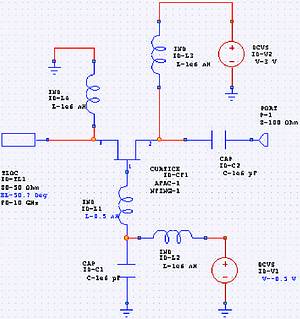
The first step is to adjust the feedback inductance and tuning stub to obtain an appropriate negative resistance. This is the small-signal resistance, not the large-signal. VoltaireXL is well suited to this task, because it automatically linearises the device at the bias point when small-signal measurements are requested. This gives us small-signal results that are completely consistent with the large-signal, we do not need the device's S parameters, and we can adjust the DC bias values if necessary to optimise the circuit. We wish to obtain approximately -100 Ω for the real part of the port impedance. This is just an initial value; we can 'tweak' it later in the nonlinear analysis. Most importantly, it must not be too high or too low; otherwise, small losses in the finished circuit could prevent the oscillation conditions from being satisfied. If one cannot obtain a resistance value in this range, the device might not have enough gain to oscillate reliably.
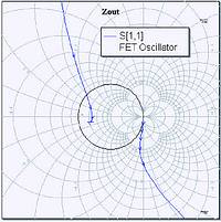
If we set the source impedance to 100 Ω, the reflection coefficient is infinite when the real part of the device impedance is -100 Ω. Therefore, we plot the reflection coefficient on a Smith chart and use VoltaireXL's 'tune' mode to maximise it. Note that the DC solution is obtained only once (unless the bias voltages are changed) so the analysis is as fast as any linear analysis, and the circuit can be tuned in real time. Figure 2 shows the result.
Device-line measurement
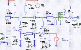
To perform the device-line measurement we need a power-impedance sensor at the port. We modify the port for swept power, insert the sensor, and set up graphs of real and imaginary parts of the impedance as a function of the excitation-source level. We also plot the real part of the output power as a function of the excitation level. (Important: The synthesised load impedance is complex, and thus the output voltage and current are not in phase. The power sensor records complex power, and the output power is the real part of the complex power. Be sure to display the real part of the power; do not display the magnitude of the power, as you might if you were calculating the power delivered to a purely real impedance.) We also insert a resistor in series with the port to prevent oscillation conditions from being satisfied; if they were satisfied, the harmonic-balance analysis probably would not converge.
The circuit is shown in Figure 3. Because of the large, 1000 Ω resistor in series with the port, the excitation level must be quite high; we sweep it from 10 to 45 dBm. This level is not, by itself, significant; we simply need enough power at the device to drive the port impedance to a low value, at which output power is maximised. Initially, we keep the values of the feedback inductor, tuning stub, and DC bias the same as in the small-signal measurement; we can tweak these quantities later, if necessary. However, if they require major modifications, there is probably an error in the design.
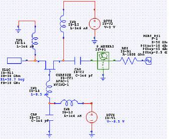
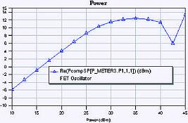
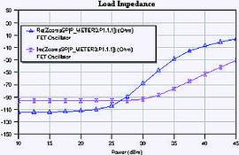
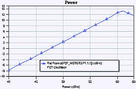
Figure 4. shows the output power as a function of the excitation level, and Figure 5 shows the real and imaginary parts of the device impedance. As we expect, the magnitude of the real part of the device impedance decreases as output power increases. At maximum output power, the device impedance is -30- j77 Ω. So far, so good, but there is still a lot to do.
Final design
First, we need to convert our ideal circuit to a practical one. To do this, we replace the ideal blocking capacitors, RF chokes, and the tuning stub with real elements. It is best to replace one or two elements at a time, rerun the analysis, and make sure that everything still works. The circuit has one more problem: the 1000 Ω resistor presents a high-impedance harmonic load to the device; in reality, the harmonic impedance would not be so high. We therefore include a quarter-wave stub to short-circuit the second harmonic; higher harmonics are probably weak enough that we need not worry much about their terminations. We convert the RFCs to high-impedance transmission lines and use series-resonant chip capacitors for the DC blocks. We also convert the tuning stub to microstrip.
When the circuit has been converted from an ideal to a practical one, we can tweak the tuning stub, feedback inductor, and gate bias to optimise the power. Little adjustment is necessary; the only significant change is a 0,1 nH increase in the feedback inductance. Although it is possible in theory to obtain greater output power than we have accepted, the characteristics are disturbing. For example, in some cases we can obtain a high output level, but the device reactance changes sign as the oscillation builds. In this case, the start-up may be unreliable. We settle for a condition where the reactance is approximately constant throughout the start-up process.
At this point, we have 13 dBm output power and a device impedance of -54-j66, so we need a load impedance of 54+j66 to satisfy the oscillation conditions at this frequency and power level. A simple series line and stub are used for the matching circuit. It can be designed quickly and easily by setting up a separate circuit and viewing the impedance on a Smith chart plot. A few manual tweaks with the tuner, and the matching circuit is complete. It is then copied and pasted into the oscillator circuit.
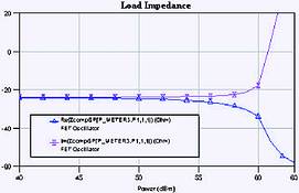
With the matching circuit installed, the analysis can be rerun. At this point, peak output power should be obtained when the load impedance is 50 Ω. With the matching circuit installed, however, the device behaves like a shunt resonance, not the series resonance that we had without the matching circuit. For this reason, preventing instability now requires a small shunt resistance, not the large series resistance we used before the matching circuit was installed. Figure 6 shows the circuit, and Figures 7 and 8 show the device output power and impedance, respectively. The peak power is 13 dBm, as expected, at a device impedance of -48+j4 Ω. This completes the basic design.
Final tests
It is always a good idea to perform a small-signal sweep of the device impedance to make sure that there is nothing worrisome in the negative-impedance characteristic. Ideally, the frequency range over which the device exhibits negative resistance should be limited and there should be no strange resonances at unwanted frequencies. A plot of this impedance shows negative resistance from approximately 6 to 12 GHz. There are no strange resonances within this range; the only loop in the characteristic is the expected one at the oscillation frequency. As long as the load VSWR is reasonably low (which can be guaranteed by an isolator or buffer amplifier), this oscillator should show no unusual behaviour.
Conclusions
A numerical device-line measurement performed on a harmonic-balance simulator is a practical method for designing oscillators. We have, incidentally, shown that VoltaireXL, from Applied Wave Research, is especially well suited for this task.
| Tel: | +27 11 314 4101 |
| Email: | [email protected] |
| www: | www.dscoms.com |
| Articles: | More information and articles about DS Communications |


© Technews Publishing (Pty) Ltd | All Rights Reserved
 printer friendly version