
All electrically conducting materials, such as metals and semiconductors, bear a characteristic electric charge just outside their surfaces. A team of researchers in Scotland is developing a novel probe that measures this charge on a microscopic scale. This unique device – called a scanning Kelvin probe – is expected to find wide use both in commerce and research.
The probe can be drawn back and forth across a surface, taking measurements to build up a three-dimensional image. It reveals minute variations in surface charge, say the researchers, offering an extremely sensitive indicator of properties such as type of material, surface defects, surface voltage and roughness.
For semiconducting samples, shining a beam of light under the Kelvin probe allows the researcher to probe material composition below the surface. The teams responsible for this project are based at the Robert Gordon University, and the Environmental Research Centre, both in Scotland.
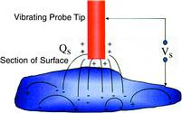
Essentially, the probe is a needle with a variable voltage which vibrates up and down just above the sample surface. If the potential of the needle and the sample are different then charge flows from one to the other. When they balance, no charge flows, and this null reading gives the charge at that point on the surface.
According to the researchers, the technique is non-destructive and versatile. Measurements can be taken rapidly, in air, a vacuum and above solutions such as water or cell-growth media, over a range of temperatures. The team has also made a portable version that can be attached to a surface with a magnet.
There are a number of possible Kelvin probe system combinations. These versions include static single probe and scanning single probe systems, both for ultra high vacuum (UHV) and ambient conditions; and multitipped scanning bio-probes for studying biological systems. The hardware involved consists of two cards that are installed in the host computer. The first is the Kelvin probe oscillator card designed by Gerrit Bruggink and Gregor Forsyth and drives the probe providing the frequency and amplitude of oscillation. It also provides a trigger that can be used by the software to ensure that the exact same part of a wave is recorded with every measurement that is performed by a data acquisition card - the second card.
The group says that this combination allows the signal to be recorded a number of times, and averaged. The software calculates the differences in potential of the surface underneath the tip to a high accuracy, less than 1000th of a volt, without touching the surface (which could damage the surface, contaminate it, or for biological surfaces, stress the biological system).
The software has been designed and written by Prof Baikie, Hazel Curtis, and Bert Lagel to provide an interface between the user and the hardware that is easy to use and understand. It synchronises the inputs and outputs so that meaningful measurements can be made, and then presents the data to the end-user in a usable fashion.
So far, the device has been used on silicon chips to detect minute traces of contaminants, image operational devices and follow surface oxidation, say the researchers. Also looked at were changes in metal catalyst surface at high temperatures, at corrosion and at work function engineering to produce surfaces with tailored properties for specific applications such as gas sensors, anti-rusting coatings and defects in solar cells. Another project involves engineering new target materials for a novel mass-spectrometry application termed 'hyperthermal surface ionisation' that allows realtime fingerprints of trace environmental gases to be measured.
Enquiries from potential agents are welcomed. For more information contact 0944 1224 26 2000, [email protected]

© Technews Publishing (Pty) Ltd | All Rights Reserved