


![]()
[Sponsored] With the continuous development of the integrated circuit industry, the connections between chips have become increasingly complex. Traditional PCB technology faces limitations in applications with higher frequency and speed requirements. Achieving stable and reliable connections between high-speed and high-density chips has become critically important. Moreover, as the power consumption of chips continues to rise, heat generation has also increased, necessitating an effective cooling system to maintain normal chip operation. As a result, the interposer PCB, a new type of PCB, has emerged.
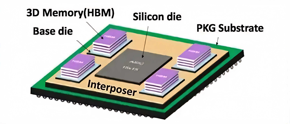
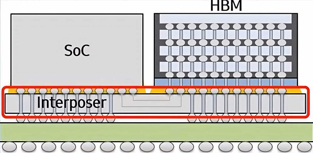
The so-called interposer PCB is a highly precise, high-layer arbitrary interconnection HDI PCB. It serves as a critical component for connecting and integrating different electronic components and acts as an intermediary layer for chip connections. It achieves electrical connections through pad leads and interconnects with the chip’s micro bumps (µBump) and the routing in the intermediary layer. The intermediary layer utilises through-silicon vias (TSV) to connect upper and lower layers.
The design characteristics of this PCB include inner layers connected to the outer layers through laser microvias and dense routing, resulting in a multi-structure with BGA connections on the top side and pad connections on the bottom side.
Interposer PCBs hold exceptional value and significance in improving various performance aspects of integrated circuits.
Firstly, interposer PCBs can provide higher connection speeds and reliability for semiconductor products. Made from high-performance materials, interposer PCBs enable short-distance, high-density connections between integrated circuits, significantly increasing chip data transmission rates.
Secondly, interposer PCB technology addresses signal integrity and power consumption issues. By utilising interposer technology, signal pins can be directly connected to the interposer layer, reducing the length of signal transmission paths, thereby minimising signal loss and enhancing signal integrity.
Thirdly, the interposer layer also serves a thermal management role, effectively reducing chip temperatures.
Finally, interposer PCB technology facilitates the connection between heterogeneous integrated circuits. By placing integrated circuits with different functions on the same interposer layer, it enables interconnections between various chips, thereby enhancing the overall performance and efficiency of semiconductor products.
In conclusion, interposer PCBs are widely used in fields such as high-performance computing, artificial intelligence, data centres, and communications. In high-performance computing systems, interposer technology can connect multiple processing chips, enabling larger-scale computing capabilities. In the field of artificial intelligence, interposer technology facilitates interconnections between different chips, enhancing the training and inference speeds of neural networks. In data centre and communication applications, interposer technology provides higher transmission rates and bandwidth to meet the demands of big data processing and high-speed communication.
As a manufacturer of high-end HDI PCBs, PCBWay [hyperlink: https://www.pcbway.com] keeps pace with market trends. In response to the urgent demand from clients for high-order arbitrary interconnection (Anylayer) HDI boards, their product research institute has dedicated itself to overcoming technical challenges, ultimately achieving the successful development of high-layer, high-order arbitrary interconnection interposer PCBs.
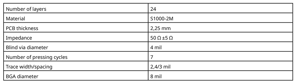
The details of this high-precision circuit product using the 24-layer, 6-order Anylayer HDI PCB, as an example, is showcased below.
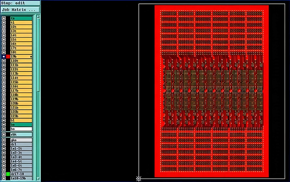
1. Product parameters
2. Product structure
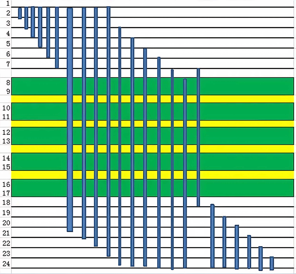
3. Technical challenges
∙ Challenge 1: The buried via PCB thickness from
∙ Challenge 2: The BGA pitch is 0,35 mm, and the distance from the hole to the conductor trace is 0,13 mm, which makes it easy for misalignment during multiple laminations.
∙ Challenge 3: The trace width/spacing is 2,4/3 mil, and it features dense routing. Below are some routing diagrams.
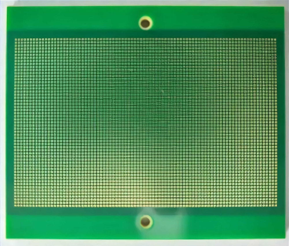
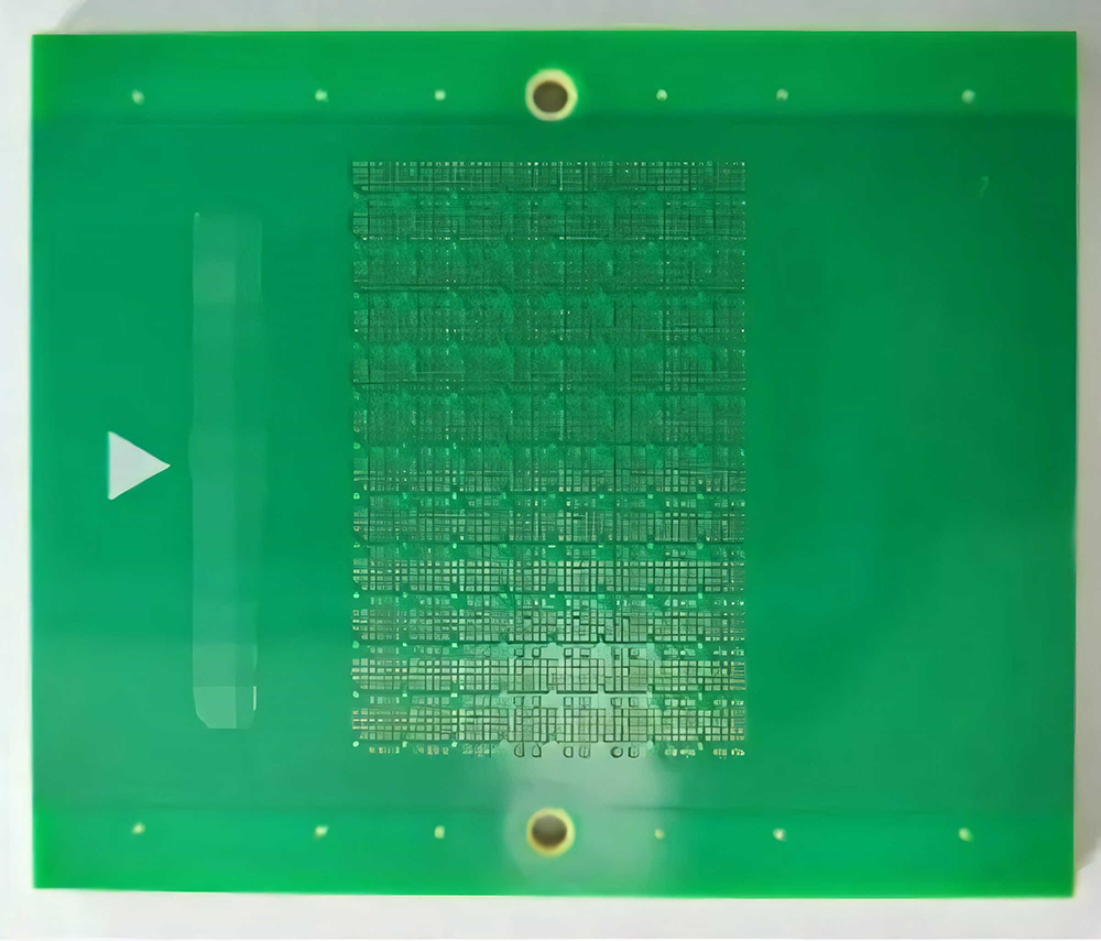
4. Finished product pictures
| Tel: | +86 571 8531 7532 |
| Email: | [email protected] |
| www: | www.pcbway.com |
| Articles: | More information and articles about PCBWay |


© Technews Publishing (Pty) Ltd | All Rights Reserved
 printer friendly version