


Once upon a time we cleaned virtually all circuit assemblies. That was until the discovery that certain chlorofluorocarbons (CFCs) contributed to the loss of the ozone layer. The industry’s most popular cleaning solvents, used to remove flux after soldering, contained CFCs. Eventually (in 1985) an international treaty known as the Montreal Protocol was signed and our industry witnessed the elimination of many CFC-based cleaning solvents. Necessity being the mother of invention, alternate cleaning materials and methods were introduced.
While these alternate materials and methods would prove effective, they paled in comparison to another technology introduced at the same time. This technology promised to eliminate the cleaning process altogether. This was the birth of ‘no-clean’ flux – a flux that left behind very little residue. So little, in fact, that the assembly would not require cleaning.
It’s interesting to note that the Montreal Protocol is one of only two treaties ratified by all United Nations member countries.
Background
Given the opportunity to eliminate an entire process step, much of the industry embraced no-clean technology. Those who were required to clean adopted new cleaning materials and methods. In the early days after the transition, both options were successful.
Little did the industry know back in the 1980s and early 1990s that the theory behind no-clean fluxes and solder pastes had a flaw. This flaw began to be more obvious as circuit assemblies became smaller and component densities became higher.
The theory behind no-clean fluxes and pastes was based on the principle that little residue would be left behind. The remaining residue would act as an encapsulator of flux activators and other ‘bad actors’. What was not widely considered when cleaning was eliminated from the electronic assembly process was the fact that, while we referred to a de-fluxing process, it can more accurately be defined as a cleaning process. When the flux was removed from assemblies, so were other residue species, including residues from board fabrication, component fabrication, the assembly process, human-transferred residues and of course, flux. When the industry stopped removing flux, it stopped removing everything.

A multitude of residue species were allowed to remain on the assembly. Fortunately, circuit assemblies were much less dense at that time
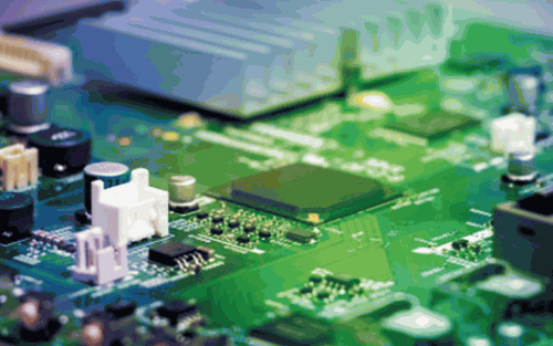
Over the 30-plus years since the introduction of the ban on most CFC-based cleaning solvents and the ensuing elimination of a cleaning process, circuit assemblies have gone through a transformation. Modern assemblies are smaller and components are smaller and closer together
Residue-related failures
Over the past three decades the percentage of assemblers cleaning boards reflowed with no-clean flux has increased. In fact, in a recent poll conducted by Aqueous Technologies,
62% of the respondents indicated that they clean assemblies reflowed with no-clean flux. While it’s not likely that no-clean flux residue is the exclusive cause of residue-related failures, the totality of residues from board and component fabrication, assembly processes and humans combine with flux residues to create the possibility of failure. Residue-related failures can fall into four primary categories:
• Cosmetic.
• Electro-chemical migration (ECM).
• Adhesion.
• Changes in electrical impedance.
While this article deals with ECM, the remedies for cosmetic, adhesion and impedance issues are identical to those for ECM.
First, let’s distinguish between two similar yet different issues: tin whiskers and electro-chemical migration. Metal whiskers
Electro-chemical migration (ECM) is a problem faced by an increasing number of assemblers. ECM manifests itself in three forms:
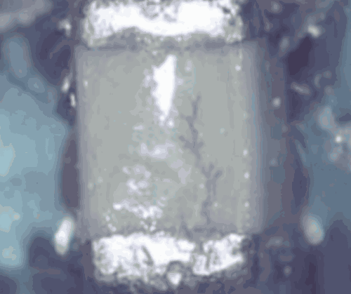
• Dendritic growth (See Figure 5).
• Parasitic leakage.
• Conductive anodic filamentation (CAF).
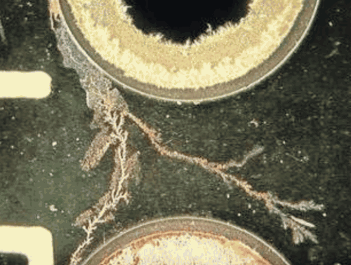
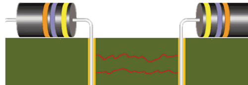
ECM is the dissolution and movement of metal ions in the presence of an electric potential, which results in the growth of dendrites (metal structures) between anodes and cathodes. In simple terms, metallic crystals connect anodes and cathodes, causing a decrease in electrical resistivity or a direct short. While dendritic growth and parasitic leakage are board surface issues, CAF occurs between the layers of a board.
Surface level electro-chemical migration requires three elements: bias (voltage), conductive residues and moisture. The elimination of any one of these elements will result in the prevention of ECM. In the case of surface ECM, the elimination of residues is the most effective method of preventing the occurrence of ECM. While the elimination of moisture will also prevent ECM, keeping an assembly away from moisture, particularly in the field, often proves difficult if not impossible. Even the best conformal coatings are permeable, allowing small amounts of moisture to penetrate to the board’s surface. ECM can occur under conformal coatings
The decision to clean or not to clean is determined by at least two factors, those being the assembly’s residue tolerance and the cost of failure. The assembly’s residue tolerance is determined in turn by such factors as:
• Conductor-to-conductor spacing.
• Component density.
• Component standoff height.
• Voltage.
• In-use climatic environment.
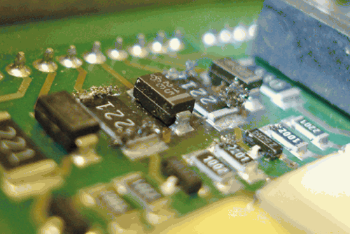
A specific volume of ionic residue between two conductors may or may not be harmful. The ratio of ionic residue to distance between conductors determines the level of ECM potential. The decrease of component spacing corresponds to a decrease in time-to-failure. Too much residue in too small a space increases ECM potential.
Not only is an assembly’s residue tolerance lowered when a single component’s conductors are close together, but a high density of components places the various component conductors close together, further increasing the likelihood of ECM. Likewise, components with ultra-low standoff heights may trap flux activators beneath the component, raising the potential for ECM (as well as solder voiding, which is common with bottom-terminated components).
Voltage plays a role in ECM. The higher the voltage, when combined with ionic residue and moisture, the greater the ECM potential.
Conductive anodic filaments (CAF)
Conductive anodic filaments (CAF) are a similar failure mechanism as dendritic growth. Whereas dendrites grow on the surface of an assembly, CAF grows between the layers. Like surface level dendritic growth, CAF requires a conducive material, electrical current and moisture. Additionally, a fourth element is required for CAF: a pathway is required between the board layers in order for CAF to form.
CAF can be a result of board fabrication failures, assembly failures and the in-use environment of the circuit assembly. First, there must be a pathway between cathodes and anodes. The pathway may be formed during the board fabrication process. As through-holes are drilled, small micro-cracks may form within the laminate. This can occur if too much pressure is placed on the board by the drill. Dull drills can increase the pressure required for drilling.
Micro-cracks may also form as a result of ‘dry weave’, an inter-filament separation within the laminate. Additionally, micro-cracks can form during thermal excursions associated with multiple reflow processes. Each time a board is exposed to extreme temperatures common in the reflow or soldering process, the expansion and contraction effect of thermal excursions can create or exacerbate micro-cracks.
The conductive material required for CAF formation is commonly the result of plating solutions used in the through-hole plating process. Both component barrels and vias are normally plated
Next, moisture is required to react with the conductive materials. Inter-layer moisture entrapment is common in multi-layer circuit boards. If left within the board, it can react with the conductive materials associated with plating solutions and electrical current to exploit the pathways and create unwanted electrical conductivity within the board
Normally, CAF formations are very thin and delicate and do not result in a major fire-producing short circuit. CAF formations can, however, have damaging consequences by draining a circuit assembly’s battery. Any unintended reduction of a laminate’s dielectric properties can reduce the assembly’s performance and reliability. CAF is less likely when the wall-to-wall internal distance (plated through-hole to plated through-hole) is wider than 350 µm–400 µm.
Unlike surface-level ECM, cleaning is not a solution to CAF – the best solution to CAF is to prevent it. CAF resistant laminates are widely available. Additionally, assembly design, through-hole spacing and voltage all play a role in CAF potential. If micro-cracks, conductive materials and short spacing are inevitable, the elimination and prevention of inner layer moisture can prevent CAF formations.
One may refer to IPC
Environmental influences
Even if a densely populated assembly is subjected to ionic residues, ECM is not a factor unless the assembly is subjected to moisture. This is true with both surface and inner-layer ECM concerns. This is where the assembly’s in-use climatic environment plays a role.

As stated earlier, voltage, ionic residues and moisture are required for ECM. The higher the ionic residue content, the less moisture is required for ECM. Conversely, the lower the ionic residue content, the more moisture is required for ECM. This is where the term ‘harsh environment’ becomes relative. With some assemblies, it would take a very harsh environment, like a down-hole application
In assemblies with high ionic residue content and high component density, normal everyday moisture such as environmental humidity may trigger ECM.
So, what is considered a harsh environment to a circuit assembly? It depends on the circuit assembly.

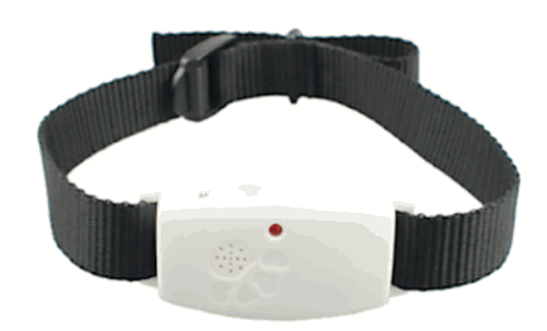
Finally and perhaps most importantly in the ‘to clean or not to clean’ consideration, one should consider the cost of failure. When a product fails, is that good or bad? If a product fails, is it costly or not? Consider two products, both containing a circuit assembly. One product is an electronic flea collar
Conclusion
As miniaturisation (of both boards and components) continues to progress, the amount of residue tolerable on and within an assembly continues to decline. Modern assemblies can tolerate less residue than their older counterparts. Today’s assemblies must be cleaner in order to prevent ECM in all of its manifestations.
The term ‘harsh environment’ is relative. Through-hole circuit assemblies from many years ago could tolerate considerably more residue than a typical modern circuit assembly. Additionally, our industry transitioned from a clean strategy to a no-clean strategy. Formerly, circuit assemblies were cleaned. Not only was the flux removed, but all other residue species were removed as well. While flux is the intended target in a cleaning application, many other residue species are also removed. Residues from board fabrication, component fabrication, the assembly process and human contamination combine with flux to create the total residue content on a circuit assembly
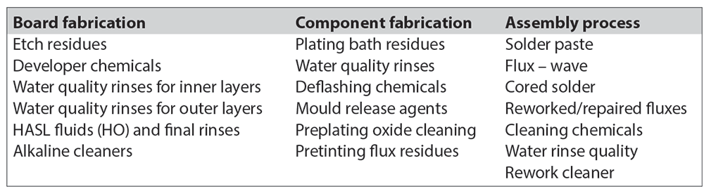 Table 1. Circuit assembly residue sources.
When the electronic assembly industry stopped removing flux, it stopped removing everything. Because of the wide adoption of no-clean processes and the reduction of residue tolerance, we now witness a perfect storm of ECM possibilities.
The removal of just one required factor for the creation of ECM (conductive residues) will prevent surface-level ECM-related failures. Our industry has two choices: provide more space between conductors, or a cleaner space between conductors. As our industry steams toward an historic expansion of electronic products as a result of the Internet of Things (IoT), wearables and the increasing electrification of automobiles, the removal of residues and the resulting increase in reliability has witnessed the cleaning process come back into the realm of conventional wisdom.
Many ask, “If I am to clean my assemblies, should I discontinue the use of no-clean flux?” I wouldn’t recommend that. The fact is, no-clean fluxes and pastes represent the state-of-the-art when it comes to flux technology. There has been little improvement in rosin and water-soluble flux technology over the past several years. No-clean flux technology, on the other hand, is considered modern, evolving and widely supported from the flux manufacturers as well as oven and thermal management companies and cleaning companies (ironically). No-clean fluxes and pastes are good soldering materials and produce high-quality solder joints. As of this moment, there is little necessity to change the flux materials.
If reliability is vital in your application, consider removing all residue species from the assembly to eliminate any opportunity for ECM-related failures, regardless of the flux type used.
While there are several cleanliness quantification techniques, sometimes one simply has to rely on the ‘sound of clean’. Consider what your ‘sound of clean’ is.
Anecdote
One of my favourite anecdotes comes from a customer that manufactures on-stage amplifiers for the music industry. Over the years, this manufacturer experienced several technical changes in their product. They migrated from vacuum tube to solid state devices. They changed from through-hole components to surface mount components. They left leaded solder for lead-free alloys. They changed flux type from water soluble and rosin-based to no-clean. The latter change ended their cleaning procedures. The no-clean approach worked well for some time, but things began to change when components became miniaturised and component density increased.
The manufacturer noticed a degradation in sound quality emanating from their amplifiers and requested that we clean their assemblies and return them for evaluation. We offered to subject the assemblies to Resistivity of Solvent Extract (ROSE) testing (an industry standard test to quantify the volume of ionic residue on a circuit assembly). They declined our offer, suggesting they had a better method of determining cleanliness. This unique cleanliness assessment required a musical ‘jam session’ using the amplifier with the newly cleaned circuit assembly installed inside it. The trained ears of professional musicians were able to hear a difference between music amplified with uncleaned circuit assemblies and music amplified with clean boards. This was the ‘sound of clean’.
| Tel: | +27 11 869 0049 |
| Email: | [email protected] |
| www: | www.mykaytronics.co.za |
| Articles: | More information and articles about MyKay Tronics |


© Technews Publishing (Pty) Ltd | All Rights Reserved
 printer friendly version