
With every new model of an electronic device, the internal components get smaller and smaller with more and more demand. Not surprisingly, this miniaturisation, coupled with increasing power throughput and heat, is significantly increasing the frequency of voiding – specifically under bottom termination components (BTC) like quad-flat no-leads (QFN). There is a growing movement to mitigate this defect, with some manufacturers specifying as close to 0% voiding underneath the ground plane as possible.
The problem is, how do you mitigate something that you can’t even see? X-ray analysis of electronic assemblies is used to measure voiding. However, there are many different settings and parameters that need to be considered before a successful measurement can be taken. This article will give an overview of how different X-ray settings can influence the quality of the final analysis.
Introduction to X-ray analysis and voiding
X-ray analysis has an interesting history. It has been around since 1895 when German physicist Wilhelm Conrad Röntgen accidentally discovered the technology. He didn’t fully understand his discovery, so he named it X-radiation for its unexplained nature. Fast-forward to today and X-rays are used in a wide range of applications and industries: medical, transportation, food and beverage, and the electronics industry.
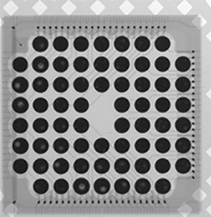
X-ray became a popular topic in the electronics industry upon the advent of ball grid array (BGA) type components (Figure 1). There are two opposing views on whether or not voiding is a defect:
1) Voiding is a cause for cracks to initiate and result in a failed solder joint.
2) Voiding can stop a crack from creating a failure.
Voiding can lead to field failures and reliability and thermal issues in electronic assemblies. It is arguably one of the single biggest challenges in PCB assembly today.
The LED, automotive, and industrial industries have developed an industry specification, according to IPC-A-610 8.2.12.4 in reference to BGA type components, that defines a failure for Class 1, 2, and 3 electronics when the voiding is greater than 25%. This specification has been adopted as the starting point for many manufacturers in regard to QFN voiding, even though there is not an industry definition of the amount of voiding that is tolerable in QFNs.
Current technology
There are many manufacturers of X-ray equipment for the electronics industry today. The technology is competitive and can be overwhelming if the capabilities are unknown.
Most important is the ability to X-ray a variety of component types with varying thicknesses and complexities. There are also machines that can create computed tomography or CT images. These images are three-dimensional and offer a comprehensive representation of what a component looks like in real space, along with where and how large the voids are within it.
Pros and cons
There are many benefits to using digital X-ray for component analysis. Radiographic analysis is a non-destructive test (NDT) method. An NDT allows for examination of the quality and function of a device without subjecting it to permanent damage, and leaves it in a condition in which the devices can be utilised. This saves not only time and money, but also allows for testing of the exact devices going into products, instead of a sample that wouldn’t be used in the field.
It is important to mention that radiation dose sensitivity is something to be aware of when using radiography to determine the quality of a product. Radiation sensitive devices can show signs of degradation with prolonged exposure to X-ray radiation. It is always important to understand what, if any, limitations there are in an electronic assembly.
Void analysis
Specific imaging is the X-ray technique that is used to determine what the voiding characteristics are for a component. Specific imaging refers to optimising the image taken to reflect the failure mode that is being investigated; in this case, voiding.
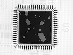
In order to determine the most accurate voiding image, exaggerating the contrast between the solder area and the voided area is paramount. If the contrast isn’t stark enough, the program will have a more difficult time to accurately detect the voids. The algorithm is built into the void software samples from the greyscales across the component to determine the difference between solder and void.
Image optimisation
When determining the voiding percentage for a particular component, quite a bit of work has to happen before the optimised image is obtained. In order to optimise an X-ray image, there are a few fundamental parameters that need to be addressed. Settings such as power, current, filters, and software algorithms are used to get an accurate representation of voiding using X-ray.
Power, current, and kV settings
The first thing to do when starting an X-ray inspection is to select the appropriate kilovolt (kV) and power/current settings for the machine based on the device being inspected. A good place to start for most semi-microelectronic devices is around 100-200nbsp;kV. Once in this range, the power/current can be adjusted until the image comes into view.
It is important to not keep the power/current on either extreme of the machine’s capabilities. If the setting is nearing either limit, be sure to adjust the kV accordingly in order to keep the power setting in mid-range.
Filtering
In some cases, the best fit exposure settings for the device/area under observation subjects the surrounding area to oversaturation. Oversaturation can be viewed as a whiteout scenario. In order to mitigate this effect, a physical filter can be used. Placing a thin copper sheet (2-10 mils) directly over the source will limit the amount of photon radiation the detector will see. Since less of this radiation is reaching the detector, less saturation will be observed in these outlying areas.
There are also a variety of filters within the machine’s software that can be applied after selecting the appropriate X-ray beam settings. For void analysis, the most important ones will be those that can manipulate contrast and sharpening.
As previously mentioned, to maximise the software algorithm’s ability to detect voids, the difference between voided areas and soldered areas must be exaggerated. Contrast filters enable a more obvious delineation between the darkest areas and lightest areas. For void analysis, this gives a larger and more obvious distinction between the voided areas and soldered areas.
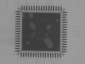
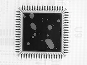
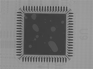
The filtering approach that highlights voided areas is to utilise a sharpening filter. This filter is similar to a contrast filter, but concentrates on localised areas as compared to filtering the entire image. Sharpening filters stretch the contrast between darks and lights at the edges of the features on the screen only. This gives the effect of more crisp edges in the image, resulting in the void algorithm more clearly defining where a voided area ends. Figures 2 through 5 show different filters and how they can affect an X-ray image.
Software
Now that an optimised image has been collected for the device under test, it is time to apply a voiding software or technique to determine the percentage area of voiding for a given area. The exact process will vary from machine to machine; however, they will all work under similar concepts.
First, the area to be measured needs to be defined by the user. In the case of QFNs, it is the ground plane and source pads. Some machines will have an automatic selection option where the machine will determine the area to be analysed based on the contrast differences across the area in view.
Once the area to be analysed is defined, the equipment’s void analysis program is selected. This is an algorithm written into the machine’s software by the manufacturer. It is set up to determine changes in contrast across the area being analysed and computes the percentage that’s voided (lighter contrast) as compared to the overall defined area. When the results display on the screen, the operator can decide if the analysis accurately detected all of the voiding. If the machine misses some voids, some software allows the user to manually detect voids and add them to the overall analysis.
Quality indicators
Now that a quality radiographic image has been acquired and void analysis maximised, it is important to ensure repeatability of the test. The settings used for each test can vary with part type and instrumentation. Keeping track of what settings are used for which components is significant.
By recording the different settings for each part type, naming the programs accordingly, and keeping a log of all this information, repeatable results can be obtained for virtually any component type. Taking the time to thoroughly optimise the image and void analysis the first time, followed by detailed documentation, will allow for future repeatability of testing. The exact process will vary from machine to machine; however, they will all work under similar concepts.
Conclusion
X-ray analysis in electronics is a safe way to assess whether or not there are defects in the process. It is a non-destructive test with many benefits and very few risks – if used appropriately. X-ray imaging is not a simple process; it is a complex technology that requires a thorough understanding of which settings and variables are important to obtain an appropriate voiding result. With the constant miniaturisation and increased heat and power of electronics, it will become more and more important to ‘Avoid the Void’.
| Tel: | +27 11 824 1427 |
| Email: | [email protected] |
| www: | www.techmet.co.za |
| Articles: | More information and articles about Techmet |
© Technews Publishing (Pty) Ltd | All Rights Reserved