


The purpose of this article is to provide customers with a guide for mounting plastic packaged high-power RF devices to a circuit board. Adherence to the methods described will enable the product to achieve good RF performance and reliable operation throughout its life.
Using this guide, customers should be able to develop mounting procedures that are compatible with their product design and manufacturing processes. These processes will produce a part with good thermal grounding for heat dissipation, good electrical grounding for stable RF performance, and reliable lead connections.
Background
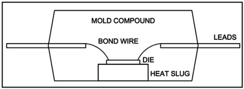
High-power plastic overmoulded packages have a unique construction – see Figure 1. In the high-power package the die is attached to a heat slug embedded in the plastic but exposed on the bottom side. The die is connected internally to leads that protrude from the package body on a different plane than the exposed portion of the heat slug.
This design enables the package to be mounted in a customer’s board so that the package heat slug can be in direct contact with a metal carrier while the leads can be in contact with the printed circuit board (PCB). This package construction and the high-power nature of the device lead to some challenges that need to be considered. These challenges include:
• Maintaining good contact between exposed heat slug and carrier for thermal transfer and electrical grounding.
• Attention to cavity height, stack-up of material and process tolerances.
• Attaching leads to PCB without overstressing.
There are several ways to mount high-power plastic packages and each has its advantages and disadvantages. It is important to understand these so that the customer can make the best decision considering cost, performance, manufacturability, and reliability.
Heat slug attach – solder-down method
The first consideration in mounting the high-power plastic package is the heat slug attach. There are two ways this can be accomplished: the solder-down method or bolt-down method. The best way to mount the heat slug is the solder-down method. When done correctly, it provides a consistent bond between the package heat slug and the carrier of the board, ensuring good thermal contact and electrical grounding for the life of the device.
The carrier is typically made of metal, usually copper or aluminium, and has a solderable surface. A copper carrier is usually plated with nickel followed by a thin layer of gold to prevent the nickel from oxidising. An aluminium carrier is typically plated by a zincation process, followed by nickel and a thin gold layer.
The solder can be introduced as either preform or paste. Solder preform, which is a pre-cut solder foil usually coated with flux, is the preferred material. This typically produces less voiding than solder paste, resulting in better thermal transfer from the device to the carrier or heat sink.
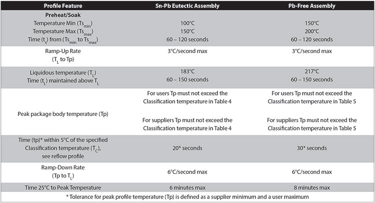
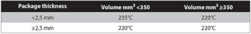
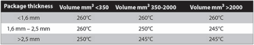
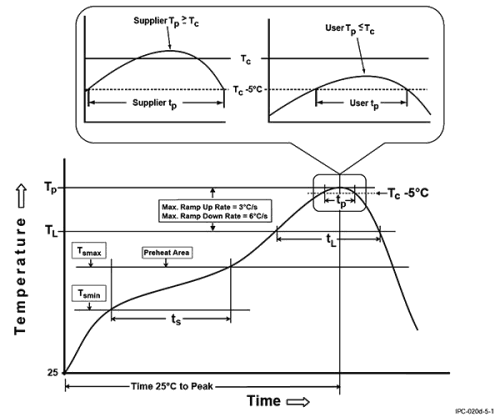
There are many lead-based and lead-free solders available, along with recommended solder reflow profiles, from the solder material suppliers. No-clean flux is recommended as this does not require an aqueous cleaning step after solder reflow. The heat slug can be soldered to the carrier as a separate process step or be done at the same time as the other components and the leads of the package are soldered to the PCB. Refer to Table 1 and Figure 6 for standard tin-lead and lead-free reflow profiles. In general, to minimise solder voiding the soak time should be extended to drive off flux and the peak temperature should be below 240°C.
Heat slug attach – bolt-down method
Even though soldering the heat slug provides the best interface, there are still customers that prefer to bolt down the part. With the bolt-down method, it is even more important to use the correct hardware, surface finish, cavity height, etc., because there is no solder to compensate for variations between the heat slug and carrier.
For bolt-down mounting the carrier is typically machined or die cast using an aluminium alloy. The surface flatness of the carrier should not exceed 0,4 mils/inch (0,4 micron/mm) and the average surface roughness (Ra) of the carrier should not exceed 32 micron-inches (0,8 microns). These values can typically be achieved by conventional machining without needing to add process steps such as lapping or polishing. Casting cannot usually achieve the appropriate flatness and roughness without an additional machining step in the area where the part is mounted to the carrier.
Using the bolt-down method it is important for the centre of the heat slug to be in direct contact with the carrier, so that there is a good thermal path directly beneath the semiconductor device. To accomplish this, MACOM recommends using a specially designed clamp that is placed on top of the part during bolt-down – see Figure 2.
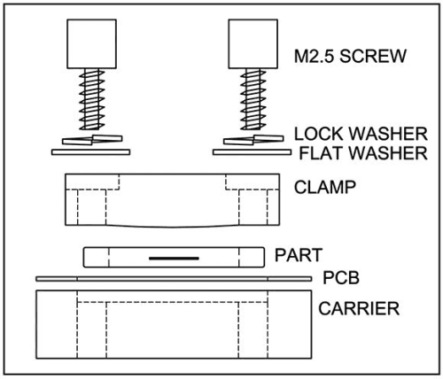
The clamp has a convex surface on the bottom that has been demonstrated to apply the appropriate force to the centre of the package, which is transferred to the backside interface between the heat slug and the carrier. The clamp is made of a polyamide glass fibre reinforced material that can handle the bolt-down stress as well as maintain its properties during the life of the device, even in different environmental conditions.
The clamp and part are bolted down at the same time using a M2.5, M3, or #4-40 screw along with a matching flat washer and lock washer – see Figure 2. A good bolting technique should be used, recommendation as follows:
1. Tighten each screw on a single part to what is commonly referred to as ‘finger tightening’.
2. Use a torque wrench to partially tighten each screw.
3. Use a torque wrench set to 5 in.-lbs. to completely tighten each screw.
The part can also benefit from the use of an interface material placed between the carrier and the bottom of the package. The interface material should have the same footprint as the part and be made of a material that is electrically and thermally conductive. Examples of materials are: thermal grease, T-GON, PGS, copper foil and indium foil.
These materials must be selected carefully considering the customer’s application to ensure they meet requirements for cost, thermal conductivity, RF stability, corrosion resistance, changing properties over time, manufacturability, etc.
Lead attach
In combination with both mounting methods, solder-down and bolt-down, the leads are soldered to the PCB. MACOM recommends that the leads be soldered after the heat slug is attached to the carrier, to minimise stress on the leads and to reduce the chance of voiding on the lead attach interface. Leads can be hand soldered or attached with solder paste in a reflow process.
In the case of hand soldering, the tip temperature should be no more than 350°C for lead-based solder or no more than 400°C for lead-free solder. Soldering time should not exceed 10 seconds per lead. The solder tip should not touch the plastic body of the part and leads should be deflected near the lead tips, not near the base. The lead deflection should not exceed 0,010 inches.
In the case of solder paste, the paste can be screen printed on the surface of the PCB. The leads are aligned to the PCB while the heat slug is aligned to the carrier and then the entire board is sent through a solder reflow process. In combination with the heat slug solder-down method, the leads and the heat slug can be attached during the same reflow step or during different steps.
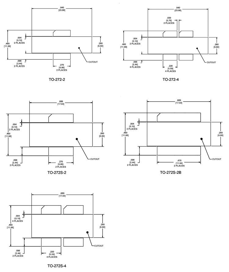
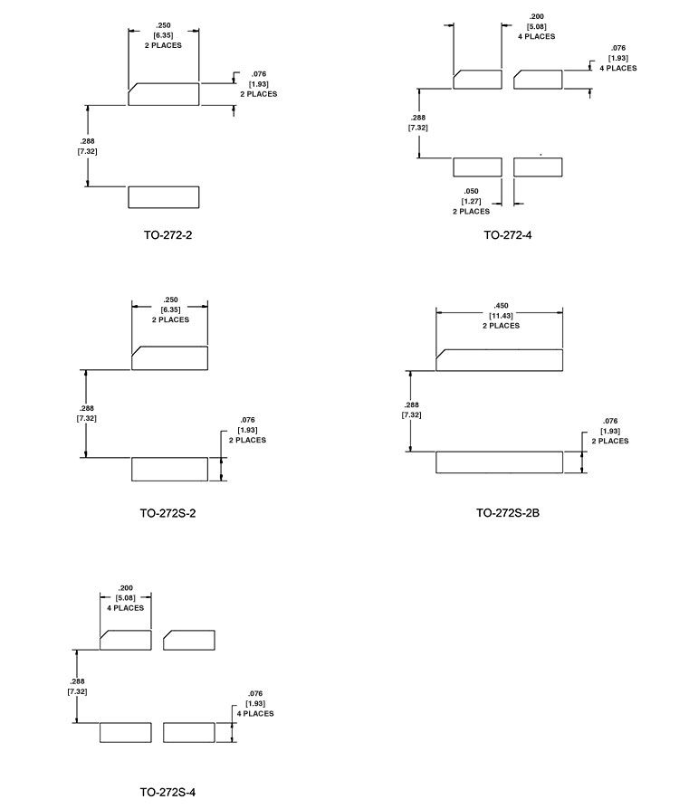
Figure 4 shows the recommended land pads that should be used to mount the various TO-272 package styles. Figure 5 shows the recommended stencil patterns that should be used to mount the various TO-272 package styles. Figure 6 shows the recommended stencil layouts that should be used for the various TO-272 package styles. As described previously, there are many different lead-based and lead-free solder options that are suitable to attach the leads. A typical lead-free solder profile can be seen in Figure 6.
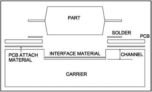
Cavity height
The distance between the top surface of the carrier and the top surface of the PCB (or solder on PCB) is referred to as cavity height. This distance is critical to ensure the heat slug of the part is making good contact for thermal and electrical grounding while the leads are attached properly without being overstressed for good RF connectivity.
There can be many layers and tolerances that affect the cavity height – see Figure 3. Some layers in the material stack-up, such as the package seating plane and interface material, bring the leads of the package away from the board. Other layers, such as PCB, PCB attach material, and solder (under leads), bring the leads closer to the board. A pedestal or channel usually needs to be added to the carrier so that the part fits properly into the board.
Each of these layers also has a tolerance that needs to be considered when determining the optimum cavity height. The best method for understanding the total variation of the assembly stack-up and to determine the correct nominal cavity height is the root sum of squares (RSS) method. To do this the customer first needs to determine the standard deviation of each of the materials in the stack-up. If these are not known, they can be derived by assuming a Cpk of 1,0 +/-3 σ process) and calculating the standard deviation by taking the one-sided tolerance and dividing it by 3.
The total standard deviation is then calculated by adding the squares of the individual standard deviations and then taking the square root of this sum. The following example will help illustrate this method.
Assume the customer is using a package with a seating plane of 0,050” +/-0,002”, a PCB with thickness 0,032” +/-0,002”, an epoxy preform under the PCB with thickness 0,003” +/-0,001”, solder under leads with thickness 0,002”
+/-0,001”, and solder preform (under package) with thickness 0,002” +/-0,0005”. The machining tolerance of the cavity or pedestal in the carrier, which can typically be held to +/-0,001”, should also be considered. The nominal protrusion of the package would be:
Nominal Protrusion = seating plane + solder preform – PCB - epoxy preform – solder
Nominal protrusion = 0,050” + 0,002” – 0,032” – 0,003” – 0,002” = 0,015”
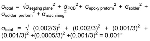
Assuming again a process Cpk of 1,0, the total variation will be +/-0,003” (3 x 0,001”). This indicates that the package (and preform in this case) will protrude 0,015” +/-0,003”. A channel will need to be added to the carrier to accommodate this protrusion.
If this number were negative, a pedestal would need to be added to the carrier. In this case the nominal channel depth should be 0,013”. It is usually better to make the channel depth smaller than the nominal protrusion to ensure the heat slug of the package is well grounded, and compensate with solder under the leads or bending the leads down slightly to the PCB. In contrast, if the channel depth is too deep the leads prevent the heat slug from making contact with the carrier, and applying additional force to bend the leads near the package body can damage the package.
Reflow profile
The most common solder reflow method is accomplished in a belt furnace using convection heat transfer. Tables 1 through 3 along with Figure 6 show a typical convection reflow profile of temperature versus time. The profile reflects the three distinct heating stages or zones (preheat, reflow, and cooling) recommended in automated reflow processes to ensure reliable, finished solder joints. The profile will vary among soldering systems and is intended as an example to use as a starting point. Other factors that can affect the profile include the density and types of components on the board, type of solder used and type of board or substrate material being used.
Thermocouples should be securely attached to the top surface of a representative component to ensure the temperature exposure is met. The profile should be recorded by data acquisition for future reference.
General soldering precautions
The melting temperature of solder generally exceeds the recommended maximum operating temperature of the device. When the entire device is heated to a high temperature, failure to complete soldering within a short time could result in device failure. Therefore, always observe the following instructions to minimise the thermal stress to the devices:
• Always preheat the device (failure to do so can cause excessive thermal shock and stress that can result in damage to the device).
• Limit the temperature in the reflow stage to the peak temperature indicated in Tables 1 through 3.
• After completing the soldering process, allow the devices to cool naturally for at least 3 minutes. Gradual cooling should be used, as the use of forced cooling will increase the temperature gradient and may result in latent failure due to mechanical stress.
• Avoid any mechanical stress or shock to the solder joints and devices during cooling.
| Tel: | +27 12 667 5212 |
| Email: | [email protected] |
| www: | www.rfibersolutions.com |
| Articles: | More information and articles about RFiber Solutions |


© Technews Publishing (Pty) Ltd | All Rights Reserved
 printer friendly version