Whenever AC has to be converted into DC, for example, to supply an electronic device with low DC voltage from 230 V a.c. mains, rectifiers are a first choice.
Irrespective of whether the necessary rectifier circuit is built up from discrete components or a complete rectifier bridge is used, Diotec can supply a suitable solution.
The company manufactures:
* Schottky-diodes for low forward losses, standard rectifiers for medium to high voltages as well as fast rectifier bridges for reduced noise generation in audio appliances.
* Zener-diodes, diacs, small signal diodes and transistors - widely used in various control circuits.
* Overvoltages caused by lightning, electrostatic discharge (ESD) or inductive switching may damage sensitive electronic components or devices. Transient voltage suppressor diodes (TVS) allow for reliable operation of such parts even in highly disturbed surroundings.
Diotec has a large production depth, from diffused silicon wafer to finished devices. This allows not only for low-cost manufacture of standard components, but also for the realisation of customer-specific solutions. Selection according to electrical parameters, bending of leads as required, or complete new development of tailor-made products according to customer needs are other services that can be easily done. Working in close co-operation with customers, it offers for that purpose, a pallet of package sizes and chips passivated by silicon-nitride and protected by polysiloxane.
Standard technology
With standard technology, once the diffusion process is complete, the silicon wafer is cut into many separate chips. Not only is the crystal lattice destroyed in the area of the saw cut, but 'dirt' (particles from the Ni/Au plating, particles from the silicon wafer, etc) impinge on the pn-junction. Etching the chips carries out the cleaning and removal of the destroyed structure. In the standard wet-etching technology, the completely-assembled diodes are put in an etching fluid and the pn-junction is afterwards coated with a protective layer. Electrical tests on the chips are thus only possible when all these production stages have been completed.
The EPOS technology
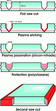
Since 1991 Diotec replaced the conventional technology of chemical etching with the EPOS-technology (EPOS stands for: etched and protected on slice). This has allowed the quality of the chips to be checked before assembly. In 1995 Diotec optimised its EPOS-technology by developing the plasma-processes. These processes are ecologically beneficial and have a minimum of chemical pollution. Processing by using plasma-EPOS technology means that the separation of the chips takes place in two stages. V-shaped cutting blades isolate the chip from one another by contouring the surface, without completely cutting through the wafer (bevelling). Plasma-etching is used for the cleaning of the pn-junction. The gas flow removes the particles, therefore they cannot settle again on the wafer. Immediately afterwards, the remaining clean lattice is passivated - also in a plasma stream of silicon-nitride. The furrows on the wafer are filled with Polysiloxane and after the curing process completely cut through. This second cut is made with a very thin saw blade through the passivation.

The silicon-nitride (Si3N4) thin films are used for insulation films in Diotec's semiconductor devices because they are dense, stable against oxidation and show very good barrier characteristics against moisture penetration. By using the plasma technology it becomes possible to deposit Si3N4 at a temperature lower than the melting point of the Ni/Au-metallisation.
Polysiloxane has optimal characteristics and is used in the semiconductor industry mainly for the passivation of ICs, eg, RAM-chips, where very low long-term defect rate is required. Polysiloxane is temperature-proof, so that the chips that follow this process can be soldered as normal and be moulded into epoxy.
Conclusion
The double passivation of the pn-junction by silicon nitride and polysiloxane results in a decisive improvement in the reliability of the components. With plasma-EPOS technology Diotec is considered a technologically-leading semiconductor manufacturer. At the centre of its daily activities are strict controls and continual improvements to the quality of its products. In the Diotec labs numerous tests are undertaken and documented. Its quality system is certificated according to DIN EN ISO 9002. Detailed information about the quality and reliability of Diotec products are covered in the Databook and in the Quality Control Handbook.
| Tel: | +27 11 458 9000 |
| Email: | [email protected] |
| www: | www.electrocomp.co.za |
| Articles: | More information and articles about Electrocomp |
© Technews Publishing (Pty) Ltd | All Rights Reserved