


This is a continuation of an article, the first part of which ran in our previous issue.
Other PI-DC results
Peninsulas and islands
Running PI-DC on designs can also reveal many imperfections that wouldn’t otherwise be apparent. Plotting the current density of power and ground shapes, for instance, makes ‘peninsulas’ and ‘islands’ of those shapes readily apparent. Figure 6 shows the current density plots of a two-layer design after running PI-DC. Notice the dark blue peninsula on the top layer and the island on the bottom layer. This unique PI-DC view highlights aspects of the design that aren’t otherwise apparent.

Care must be taken before assuming a shape that is unused for PI-DC of a particular voltage isn’t needed; that shape might be used for another voltage or for AC power delivery (attached to capacitors). Putting small resistors in place of the capacitors during a PI-DC simulation and checking the corresponding current distribution allows a designer to see if an island or peninsula in a power shape is used for AC power delivery (note the DC results will be invalid for this simulation).
Current islands and peninsulas are especially troublesome in that they will have specific resonant frequencies, possibly causing failures only when certain conditions exist. The failures may appear random and thus extremely hard to troubleshoot, a recipe for delayed validation.
Return paths
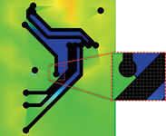
The current density and voltage plots of the power and ground shapes can also reveal problems with their design in efficiently channelling current between the power source and load(s). The voltage plot of the top ground shape in Figure 7 makes the inefficiency of the paths between the sources (the voltage regulators, or VRs) and the load (FPGA) very clear.

There may be valid reasons for not having a straightforward path between the VRs and FPGA, but PI-DC will highlight the inefficiencies so they can be addressed, if possible. As a side note, it should be pointed out this shape is problematic for AC power delivery, possibly inducing excessive inductance into the ground path and corresponding ‘ground bounce’ (inductance increases with loop area).
Of course, the designer has to take care to also view their ground shapes in the context of their use as return paths for high-speed signals, which may not overlap with their function as DC return paths. Ground (and some power) shapes that look unnecessary for DC power distribution purposes may be critical for signal integrity. But even in that context, islands and peninsulas should be avoided and only designed in when no other option exists. PI-DC often nicely highlights these unwanted shapes where they exist.
Plane breaks
Another example where a PI-DC current density plot can be uniquely insightful is shown in Figure 8. In this example, a small break in a ground plane is very obvious; the current density colour abruptly changes from green to blue at the break. This makes a profound difference in the DC power delivery of that shape; it’s doubtful the problem would be identified without using this PI-DC results view.
Measuring resistance
Some non-intuitive aspects of PI-DC are worth noting. The DC resistance of a path depends not only on the width of the path, but the length also. A DC path can be narrow if it isn’t too long without significant effect on the power delivery. For instance, paths (b) and (d) of Figure 9 have approximately the same resistance (in case d, there will be some added resistance due to the width transitions).

To understand the DC resistance of shapes, the concept of squares is valuable, as shown in Figure 9. This will allow flexibility; a DC path may be constrained to a narrow width if it is only for a short distance, and widening the path as much as possible in wide open spaces can compensate for necessary restrictions. Using the same width for a power delivery net along its entire length is inefficient, doesn’t give the best power delivery available, and uses unnecessarily large power shapes.
Figure 10 illustrates four power shapes with very different forms, all having approximately the same overall resistance (width transitions will increase the resistance somewhat in the third case). PI-DC gives designers options to modify the PDN shapes to meet the power delivery requirements in the most efficient manner.

Why do designs with errors work?
Running PI-DC on existing designs will inevitably find many ‘errors’ in the designs. Some users report finding errors with virtually every design analysed with PI-DC. How do they work if they’re so broken? Two primary factors permit faulty designs to function, even with flaws in their PI-DC construction:
1. DC power delivery has historically been conservative. To determine the correct width of a conductor for a given current, IPC specifications call out the width, dependent on the allowable temperature rise. Digital designers typically don’t have reliable data on how much temperature rise is appropriate, so they use conservative values, probably based on past experience, or provide “as much copper as is available.” If they have doubts as to whether it’s enough, they count on checking the voltage(s) during validation. If the design meets the requirements, that adds to their experience, and they use that as a guideline for future designs. In the absence of failing designs, there is no way for a designer to know if they can reduce the amount of copper dedicated to power delivery, so they grow conservatively. There is enough margin in the design to accommodate flaws, even significant ones.
2. Peninsulas or islands don’t negatively affect the DC power delivery, but can affect AC power delivery and/or signal integrity in a seemingly random manner. They are an indication that a design can be improved, but may not cause a design to fail for DC power delivery. They do present other especially problematic issues for AC power delivery and signal integrity in that they can resonate at particular frequencies. If those frequencies are excited in the shape, excessive AC noise can be induced on the PDN, or, if there are signals adjacent to the shape, it can introduce significant noise on those signals at its resonant frequency or frequencies, causing logic failures. In either case, the failures will depend on the existence of the particular resonant frequencies and may appear random, or only occur in very particular circumstances, making them extremely hard to replicate, troubleshoot, and correct. It is much wiser to take steps to preemptively mitigate these particularly mischievous issues.
Perhaps ‘imperfections,’ ‘areas for improvement,’ or ‘non-idealities’ would be better terms to use than ‘errors.’ With today’s emphasis on battery life and cost savings, being overly conservative or allowing flaws in a power shape such as peninsulas can make the difference between a failed or successful product. PI-DC not only gives information about whether a PDN is adequate, it can inform about whether power delivery shapes are necessary.
Limiting current
An important consideration in the design of a PDN is providing for unplanned circumstances. The designer has to be aware that, in the case of a catastrophic increase in current (a short to ground, for instance), an optimised power shape might not be able to absorb that extra current and cause a failure in the design. Some means of limiting current flow in the case of catastrophic errors needs to be provided if those might be encountered (power going to any connector that might be shorted during installation, for instance).
Determining via size and number
A rule of thumb commonly used for power delivery is to have enough vias such that their cross-sectional area is the same as, or larger than, the power shapes they are connecting. Experience indicates this is sufficient, but a PI-DC tool can indicate whether this is necessary.
Using excessive vias, or excessively large vias, causes routing restrictions in all the layers above and below the transition, and should not be done lightly in most of today’s designs. Unnecessary vias in one power shape may impact another power shape on other layers.
A PI-DC tool gauges the effect of vias on the PDN. Figure 11 shows seven vias (circled, labelled a to g) in a power delivery design. Careful examination reveals there is a significant colour change in three of the vias – a, b and d – indicating a corresponding voltage drop due to each of these three. Probing the exact voltage at the top and bottom of these vias (a common capability of PI-DC tools) allows the designer to determine if the via size and number are adequate and necessary.

As previously explained, there is some ambiguity in the exact dimensioning of vias in simulations, so care must be taken to account for plating thickness effects, for instance. Note that vias are typically represented as lumped elements, assigned a resistance as a function of the vias’ diameter and length, and are typically not solved as complex columns within the solver, making simulations much faster, while not sacrificing significant accuracy.
| Tel: | +27 12 665 0375 |
| Email: | [email protected] |
| www: | www.edatech.co.za |
| Articles: | More information and articles about EDA Technologies |


© Technews Publishing (Pty) Ltd | All Rights Reserved
 printer friendly version