


Designers of rechargeable battery-powered equipment want a charger that minimises charge time with maximum charge current, by maximising the power taken from the supply without collapsing the supply. Resistances between the supply and the battery pose a challenge to this goal. This article explains how to design the charging circuit to achieve the maximum power from the adaptor despite the undesired resistances between the supply and battery.
General operation of a switch-mode charger
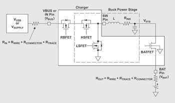
Figure 1 shows a circuit model of a buck converter-based charger illustrating all of the non-ideal resistances, including the inductor’s DC resistance (RIND). The input supply voltage to the charger IC at its VBUS or IN pin is from a typical USB port or a wall adaptor. This model will be used to derive the minimum supply voltage for a given battery regulation threshold.
Review of Li-Ion charger operation
As shown in Figure 2, the charger works in three main phases of operation, depending on the battery voltage:
1.Low battery voltage signifies a deeply discharged battery. Hence, it must be charged by a low value of current until it is brought to the threshold value, VPRECHG. This is known as the precharge phase.

2. Once the battery voltage increases to a certain threshold (VPRECHG), the prescribed maximum charge current is allowed to flow. This current is maintained by a regulation loop known as the current-regulation/constant-current phase.
3. After the battery voltage increases to the set regulation voltage and the charge current has tapered down, the battery is fully charged. While the charge current is tapering down, the charger operates in voltage-regulation/constant-voltage mode. The typical regulation voltage is 4,2 V for Lithium-Ion (Li-Ion) cells.
For fastest charge time, the charger must provide the maximum charge current for which it has been set, until VBAT = 4,2 V.
To determine the minimum value of the input voltage (VBUS_MIN) permissible, the designer must consider the following:
Operation headroom between VBUS and VBAT to reach a target charge current.
Switching regulator’s maximum duty cycle.
Operation headroom
The resistance in the MOSFETs and the inductor generates a voltage drop as current flows. If the voltage difference between VBUS and VBAT is too small, the target charge current cannot be achieved. For example, if VBUS is 4,3 V, VBAT is 4,2 V and total resistance from BUS input to battery is 150 mW, the maximum current to the battery is 660 mA.
Switching regulator maximum duty cycle
Realistically, no high-side NMOS buck converter can reach 100% duty cycle. There is always dead time to avoid shoot-through during HSFET/LSFET turn-on/turn-off. If the duty cycle exceeds the maximum value, the switching regulator will skip some LSFET turn-on pulses to maintain average output current/voltage.
Calculating VBUS_MIN threshold
The VBUS_MIN threshold is the minimum BUS pin voltage required to support the target maximum charge current and keep the duty cycle below the buck converter’s maximum duty cycle.\
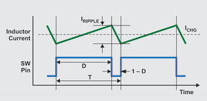
Figure 3 shows the inductor current and switch-mode voltage of a buck converter operating in the continuous-conduction mode (CCM). VBUS can be derived as follows via ripple-current calculations for the inductor.
[Equation 1]
On the inductor current rising edge:
[Equation 2]
On the inductor current falling edge:
[Equation 3]
Since the ripple current is the same, the VBUS equation can be derived:
[Equation 4]
Equation 4 can be simplified with some assumptions:
• With L = 2,2 μH, the ripple current at 96% duty cycle is less than 300 mA. (One is considered as average current.)
• With maximum duty cycle of 96%, (1-D) / D is only 4,2% compared to the second item in the equation. Therefore, the third item can be ignored.
The VBUS_MIN threshold is the VBUS voltage at maximum duty cycle:
[Equation 5]
If VBUS falls below the calculated VBUS_MIN threshold, then the battery will not fully charge.
Minimum USB supply voltage
It is possible for the input voltage to the charger to fall below the permissible value when USB adaptors are used, due to input line resistance.
The USB specification states that the output to the device from a low-power port can be as low as 4,1 V under full load, after passing through all hubs and cables.
Assume that the input supply in Figure 1 is a USB port providing VUSB of 5 V with zero resistance in series, and RIN is the lumped resistance of the cable, connector and PCB trace. The charger is modelled as an ideal buck converter that can reach 100% duty cycle.
The input voltage (VBUS) at the charger must be above the battery charging regulation threshold VBATREG (typically 4,2 V). Assuming that the minimum to which VUSB falls is 4,75 V:
[Equation 6]
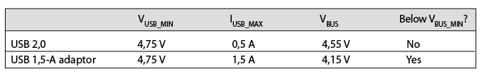
With resistance from the USB supply to BUS pin of RIN = 400 mW, Table 1 shows the minimum VBUS voltage from a USB2.0 port and USB 1.5-A adaptor.
At maximum duty cycle, VBUS is close to VBAT, so IUSB ≈ ICHG. Equation 5 can now be expanded to determine the minimum input supply voltage for a given charge current:
[Equation 7]

Equation 7 can be used to determine how low to make the cable resistance and connector (for instance, by selecting a higher quality cable and connector), or how wide/thick to make the PCB trace to avoid excessive voltage drop at the charger’s BUS pin. This maximises the adaptor’s power for charging the battery.
Input voltage-based dynamic power management (VIN-DPM)
If multiple adaptors and/or cables and/or connectors are expected to be used, it may be difficult to design for all line-resistance scenarios.
A charger with VIN-DPM prevents the input voltage from crashing regardless of input line resistance.
What is VIN-DPM?
VIN-DPM is an analog loop included in many TI chargers. Its purpose is to extract the maximum amount of current available from the supply without crashing the adaptor, ie, the input current (and therefore the resulting charge current) is limited in order to maintain supply voltage at VIN-DPM. This feature can be used when a USB port is one of the input power sources.
Operation without VIN-DPM
Consider using a charger without the VIN-DPM protection, as shown in Figure 4. As the system load current and battery charge current increase, the input current also increases, hence the drop across the supply resistance increases. The voltage seen at the charger’s input pin is less than the rated output voltage offered by the supply.
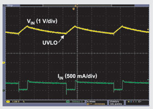
Also, the supply (voltage source) has a compliance limit on the amount of current it can produce. When a load current is drawn such that the input current required to maintain the sum of charge current and load current is beyond the capability of the supply, the input voltage starts to fall because the input capacitor discharges due to the high current demanded.
When the input voltage hits the undervoltage threshold, the charger turns off. During this off time, the input voltage recovers as the input capacitor recharges. Once it rises above the UVLO, charging begins again. Once the charger turns on, the same cycle repeats, resulting in non-ideal on/off pulsing in the charge current.
Benefits of VIN-DPM
A charger with the VIN-DPM feature prevents the non-ideal pulsing of charge current by limiting input current. Specifically, as the input voltage drops and hits the set VIN-DPM threshold, the VIN-DPM function activates to reduce the input current to a smaller value. This prevents the input voltage from crashing to the under-voltage point.
Adaptors typically supply currents between 100 mA and several amperes, and the latest USB ports can supply up to 1,5 A and higher. When using a charger with VIN-DPM, portable equipment manufacturers can optimise the charger for adaptors and USB ports having a certain output power limit, such as a current limit.
VIN-DPM allows operation with other lower-cost adaptors, USB ports and/or the cables in between. For example, a smartphone with a charger having VIN-DPM would be able to extract maximum power from a 1,5 A USB port without collapsing the port, even if a low-cost, highly resistive USB charging cable is used.
Figure 5 shows the effects of two different input resistances from the power supply to the IC. The evaluation circuit was a battery charger like the bq24192, bq24250, bq24260 or bq24295, configured for 1,5 A input current limit, 2,0 A charge current and 4,76 V VIN-DPM threshold.

In both cases, charging continues and the adaptor does not crash. However, in Figure 5(b), the VIN-DPM circuit reduces the input current limit in response to the voltage drop across the series resistance. With reduced input current, the charger will first reduce the charge current and then the system load current.
Conclusion
Resistances between the supply and charger can prevent the charger from pulling the maximum power from its supply without collapsing the supply and hitting the charger’s under-voltage lockout. An equation can be used to determine the minimum supply voltage required for a charger to provide the maximum charge current from a given supply adaptor.
Additionally, the VIN-DPM feature allows the use of a variety of adaptors and/or power connections without fear of collapsing the adaptor voltage, as it dynamically reduces the charger’s input current limit.
For more information contact Erich Nast, Avnet Kopp, +27 (0)11 319 8600, [email protected], www.avnet.co.za


© Technews Publishing (Pty) Ltd | All Rights Reserved
 printer friendly version