
Electronics are now a fundamental part of our everyday lives. As we become more technically competent and dependent, so our demands and expectations grow.
Today, as consumers, we now expect increased functionality and reduced form factor with each new generation of product development. This relentless demand for product efficiency, however, is starting to stretch manufacturing design rules, forcing different component architectures and strategies to be considered.
As part of this, it is only natural to take existing technology and try to scale it for future requirements. In this respect, companies are now experimenting with 0,3 mm pitch chip-scale package (CSP) component designs as an extension to yesterday’s ‘state of the art’ 0,4 mm pitch CSP technology.
From an assembly perspective, whilst there are many facets to the stencil printing process, it is the stencil aperture area ratio that fundamentally dictates what can and cannot be printed. This is a simple ratio rule (Figure 1) between the surface area of an aperture wall and the surface area of the aperture opening (which effectively defines the landing area of the pad onto which the solder paste is to be printed).
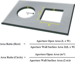
If the surface area of the aperture wall exceeds that of the aperture opening then the solder paste will want to ‘stick’ to the aperture wall more than the pad, resulting in a contaminated aperture and an incomplete solder paste deposit. Conversely, if the aperture opening area is greater, then the solder paste will favour ‘sticking’ to the pad rather than the aperture wall, leading to a more complete printed deposit.
From this, it can be appreciated that as the stencil aperture area ratio decreases, the chances of successful printing with full deposits become slimmer. A typical paste transfer efficiency curve showing this relationship is shown in Figure 2.
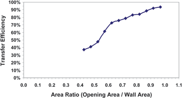
For many years the design of stencil apertures has been based around the original IPC7525 specification which recommended that aperture area ratios should be greater than 0,66 for acceptable stencil printing (to achieve in excess of 70-75% transfer efficiency).
The ‘historical’ transfer efficiency curve shown in Figures 3 and 4 is generally accepted as a point of reference for where the industry was back in the nineties, and is still used widely today as a baseline for setting up a process. In recent years, though, a tremendous amount of research and development has taken place with solder paste materials, stencil technologies and process enhancements to improve paste transfer efficiency.
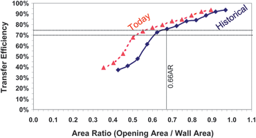
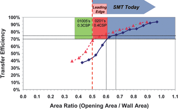
Taking all these developments and improvements into account, with a fully optimised process the ‘Today’ paste transfer efficiency curve of Figure 3 is a truer reflection of where the SMT printing industry is today.
Whilst some of these technology advancements are recognised in the latest IPC 7525 specifications, it is clear that we are operating on the boundaries of existing area ratio rules for today’s leading-edge components (Figure 4).
Although many individual operators are able to achieve a stable, capable process with these fine pitch components, extreme care and control over materials are required. In the future, if trying to incorporate 0,3 mm pitch CSP’s into existing processes, stencil apertures with area ratios of approximately 0,40 to 0,45 will be required, which are significantly beyond today’s printing rules.
As a result of this, the development reported within this article focused on the use of a new active squeegee technique to essentially shift the knee of the transfer efficiency curve – to open up the possibilities of using lower area ratio apertures and hence satisfy the needs for 0,3 mm pitch CSP printing.
Experimental setup
Equipment background
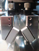
In the development of an ‘active’ squeegee system (Figure 5), the squeegee assembly contains electronics to assist the deposition process during a print stroke. The squeegee assembly can also be used in ‘traditional’ mode without activation to aid direct on vs. off comparisons when required.
Previous work by the current authors has clearly highlighted benefits for improving solder paste transfer efficiency with low area ratio aperture designs using basic test vehicles. In this study, attention was purely focused on assessing the suitability for 0,3 mm CSP component geometries.
Test vehicle
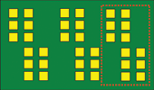
The test vehicle used throughout this investigation was constructed of FR4 and measured 148 x 114 x 0,94 mm. The layout consisted of 36 individual 0,3 mm pitch CSPs with each array containing 424 mask defined pads. Due to data set size constraints, only the 12 components on the right hand side of the board were analysed; this still represented some 5088 data points per print.
Test stencils
Printing trials were conducted with three separate 100 micron thick laser cut metal stencils having circular aperture geometries of 160, 180 and 200 microns, (equating to area ratios of 0,4, 0,45 and 0,5).
Equipment and materials
A DEK Galaxy automatic stencil printer fitted with an ‘active’ squeegee assembly was used for all print experiments. Printed deposits were measured for volume, height and area using a CyberOptics SE300 fitted with a micropad sensor. During the print cycle the test substrates were secured in place with a dedicated vacuum tooling plate.
The same squeegee assembly together with 170 mm long blades was used for all testing in both the standard and activated print mode. Prior to each test run the squeegees were automatically calibrated. An industry standard lead-free type 4 solder paste was used for all printing.
Test procedure
For experimental integrity all tests were performed with the identical machine, operator, process parameters (Table 1) and material set (excluding stencil).
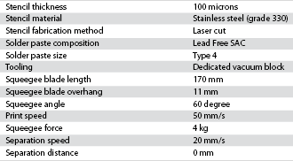
Eleven consecutive prints without interruption were made; the first substrate was discarded and the subsequent 10 substrates measured for height, area and volume. For each stencil two runs were conducted, with and without the squeegee system activated.
Results
Height, area and volume data was collected using a CyberOptics SE300 system for each of the three stencils, both with the squeegee activation off and on. This data is presented here in stencil aperture size order.
160 μm aperture stencil (0,4 area ratio)
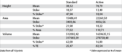
Table 2 numerically sets out the height, area and volume data generated for the stencil with 160 micron apertures. It is clear that the active squeegee has had a positive affect with the mean deposit height increasing from 38 microns to 74 microns, percentage area printed increasing from 77% to 110% and transfer efficiency increasing from 25% to 82%.
However, it is the histograms (Figure 8) that give a clearer picture of the underlying print quality trends. In the volume histogram plot it can be seen that with the standard squeegee process the data is centred around a mean of 25%, and this is to be expected with a standard material set and printing process.
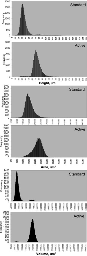
Activating the squeegee significantly improved paste transfer efficiency to 82%, but whilst the mean number is more than acceptable, the small tail to the left of the histogram curve does indicate that there were a few deposits light in volume which would represent a manufacturing defect in a real life production process. A similar trend can be detected in the height histograms as well.
The photographic images in Figure 7, taken from the 6th print in each run, clearly show the improvement in paste transfer efficiency. Nonetheless, the data indicates that not all deposits were being fully formed even with the activated squeegees, and therefore this aperture design cannot be considered as an optimised solution for 0,3 mm CSP printing.
180 μm aperture stencil (0,45 area ratio)
Table 3 (see page 19) shows the statistical results for the 180 micron aperture stencil. It can be seen that the mean responses for both standard and active squeegee runs were much closer to theoretical values (100%) compared to the first, 160 micron aperture stencil.
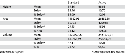
However, the standard deviation figures reveal that the ‘standard’ squeegee process is still not capable. The twin peaks of the height and volume histogram plots (Figure 11) indicate that whilst many of the apertures have printed successfully there are still a significant number of light and incomplete deposits.

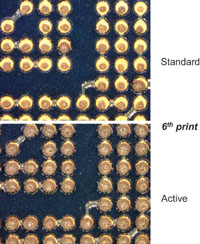
In contrast, the data for the active squeegee is tightly centred around the theoretical, indicating the process is capable of printing apertures with area ratios of 0,45. The photographic evidence also supports this (Figure 9): the images recorded from the standard squeegee process highlight the random nature of the incomplete deposits, whereas the image from the active print shows no visible defects.
200 μm aperture stencil (0,50 area ratio)
The statistical results from the tests run with the 200 micron aperture stencil are shown in Table 4. The data indicates that the standard squeegee process is capable of printing with apertures having an area ratio of 0,5. The mean values are close to theoretical (100%) with an acceptable standard deviation.
A word of caution has to be made though because a very faint left hand tail in the volume and height histograms does indicate the process is suffering from a few occasional light deposits.
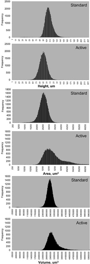
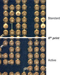
Conversely, the results with the active squeegee indicate that this particular process has gone beyond a stable state. The active squeegee process has tended to over-fill the deposits and this can be seen with the increasing right-hand shoulder in the area and volume histogram plots. This can also be clearly seen in the photographic evidence shown in Figure 10 with the active squeegee print exhibiting bridging of the deposits after six prints.

Discussion
The experimental work reported here was conducted with the intention of providing stencil printing recommendations for a 0,3 mm pitch CSP assembly process. The results indicate that there are two potential paths towards achieving a successful print process.
The data produced with a standard squeegee process when using a stencil with 200 micron apertures suggests a capable process can be achieved. Caution however must be exercised if considering this as a production option.
The histogram plots indicate that random missing/light deposits can still occur and this would need careful monitoring. The cause behind this effect is not truly understood, but as more experience is gained with ultra fine-pitch printing and challenging aperture area ratios, this phenomena is becoming more prevalent.
From a stencil perspective, 200 micron apertures on a 300 micron pitch (when considering a 100 micron thick foil) is at the limit of manufacturers’ capabilities and leaves the print operator with an aperture interspace of only 100 microns. This design constraint could encourage excessive bridging within printed deposits, and therefore a production process would require a high frequency of cleaning, resulting in a high-overhead, low-volume solution.
More encouragingly, the active squeegee produced a highly capable and centred process with a 180 micron aperture stencil design. With an aperture interspacing of 120 microns the tendency towards bridging is lessened. Indeed, in this experiment, (albeit with a very limited sample size), it was possible to perform 10 consecutive prints without any stencil cleaning and maintain print deposit integrity.
This would provide a very satisfactory manufacturing solution if this could be carried over into a production environment. In addition, the active squeegee print runs did not suffer with the random light phenomena exhibited in the standard squeegee tests. As more experience is gained with active squeegees this is becoming a key benefit of the technology.
| Tel: | +27 11 609 1244 |
| Email: | [email protected] |
| www: | www.zetech.co.za |
| Articles: | More information and articles about ZETECH ONE |

© Technews Publishing (Pty) Ltd | All Rights Reserved