


In launching its AUDO MAX TriCore family, Infineon has introduced three new series of the TriCore microcontroller in 90 nm technology onto the market, which are suitable both for high-performance and cost-sensitive applications.
AUDO MAX is the fifth generation of TriCore 32-bit microcontrollers, of which to date over 30 million units have been shipped and which are used in deeply embedded systems for controlling electrical drives, industrial machines, mobile work equipment and in the drive trains of many vehicles.
Besides the technical features such as hard real-time and a wide selection of integrated function modules, the thing all these fields of application have in common is the demand for long-term availability, maximum reliability and compliance with functional safety requirements.
The example from the field of drive technology described in this article illustrates the performance and flexibility of the TriCore CPU and on-chip peripheral units.
Requirement for motor control
Modern electrical drive systems would be inconceivable without smart and sophisticated frequency inverters. In Europe, some four million such inverters are produced each year. The growing requirements in terms of speed, precision, energy efficiency and communication call for efficient and flexible microcontrollers.
‘Single-chip’ inverters promise cost reductions. The 32-bit TriCore from Infineon was specially designed for this class of embedded real-time systems with a high interrupt load coupled with high processing power.
A decisive factor for the overall performance is the interaction of the processing kernel with the peripheral units. The block diagram in Figure 1 shows the processing kernel at the top and its connection to the program and data memories. The internal Flash is connected via a high-speed 64-bit bus.

The TriCore offers numerous smart peripheral modules. In this regard, the most important modules for the inverter functionality are the GPTA timer unit and the A/D converters. Other modules include the system timer (STM), the I/O ports, the serial interfaces – for example for connecting angle encoder – and the MultiCAN communication module. These units are connected by means of a 32-bit system peripheral bus (SPB).
A second, small 32-bit RISC processing kernel – the peripheral control processor (PCP) – is also connected to this bus. The PCP is specifically designed for processing time-critical, short interrupt functions and has fast direct access to the peripherals via the SPB.
It can pre-process and process the input and output signals and subsequently transfer them to the TriCore CPU, or work independently of the CPU. A TriCore microcontroller is thus always an asymmetrical dual-core processor for which the PCP relieves the TriCore CPU.
Frequency inversion and PWM control
In principle, the frequency inverter consists of a rectifier, which feeds a direct-current or direct-voltage intermediate circuit, and an inverter, which is in turn fed from this intermediate circuit.
The inverter consists of a bridge on the basis of MOSFETs (metal oxide semiconductor field effect transistors) or IGBTs (insulated gate bipolar transistors), whose output voltage is regulated by pulse width modulation (PWM).
In a number of control circuits, the microcontroller determines the rotor position of the motor via a resolver or encoder, measures the phase currents of the motor and calculates the PWM signal in accordance with the specifications for torque and angular velocity. PWM frequencies of 4 and 20 kHz are common.
With the TriCore, the PWM signal is generated by the GPTA – a generic timer unit that can be flexibly adapted to the specific requirements of the inverter or an operating mode. Depending on the application, emphasis may be on reducing torque ripple, minimising power loss, ensuring the quality of the output current, avoiding current or voltage harmonic interference as well as noise generation and other control algorithms.
In conjunction with the 12-bit A/D converters and the DMA controller, the GPTA forms the heart of a complementary 3-phase PWM signal generator. To this end, the GPTA provides modules made up of timer cells which, by means of configuration, can be interconnected with each other to produce the required function.
The configuration takes account of the necessary delay times when switching off and on in order to protect the half bridges. These time lags can be set separately and, if necessary, also controlled dynamically during run time.
Whilst a simple PWM signal only requires two timer cells, a complementary 3-phase PWM signal requires 26 cells. A GPTA module has 64 cells, meaning that sufficient resources are still available in order to generate further signals for the application.
In addition to the PWM signal generation, the synchronous measurement of the phase currents with at least two ADCs is important for the application. To this end, the GPTA generates a trigger event, which initiates a conversion on both ADC modules exactly in the middle of the period.
However, instead of defining just the two phase currents, it is also possible to measure all the analog input signals required for the controller in an equidistant scanning sequence across multiple channels. A scanning sequence such as this with up to 16 channels is supported by the ADC modules of the TriCore.
Cycle-precise synchronisation of multiple ADC modules can be parameterised. If, however, the number of ADC modules is less than the number of required input variables to be measured synchronously, it is possible to determine the value arithmetically by interpolating two measurements.
Figure 2 illustrates the time response within a PWM period. For space reasons, only the high-side and low-side signal of a PWM phase are illustrated. In this example, the ADC trigger initiates a scanning sequence with 10 channels on eight (0-7) input signals.
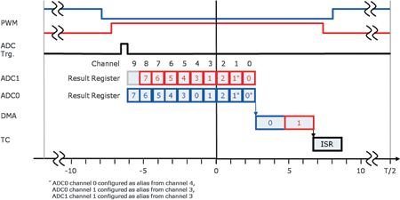
The time of the trigger event is chosen such that the scanning for the phase currents ensues on channel 2 of modules ADC0 and ADC1 precisely in the middle of the period. Input signal 1 is – as described – measured and totalled upstream and downstream from channel 2. The signal on ADC0 channel 0 is also measured and totalled up twice.
This totalling is part of a hardware-based, configurable data reduction filter within the ADC module, which permits a totalling of up to four values of a channel. As a result of the described configuration, five input variables are measured virtually at the same time.
After the scanning, another event triggers two DMA transmissions, which transfer the ADC values into the local data memory (LDRAM). Reading the values directly from the TriCore would of course be possible. Access via the bridge between LMB and SPB requires a number of clock cycles, however, and would delay the program execution on the TriCore CPU.
It is better to leave the DMA controller to transmit the ADC values in the background into the LDRAM, from where four ADC values can be read with a double-word load instruction into the CPU register in a single clock cycle. The subsequent interrupt service routine (ISR) comprises the control algorithm.
An optimised implementation of the Park and Clarke transformations mostly used and the space vector modulation (SVM) requires less than 2 μs on a TC1782 with 180 MHz CPU clock frequency.
Less than 9 μs after measuring the phase current, the controlling has been completed and the PWM values for the next period written. With further application-specific algorithms, such as the processing of the encoder signals, although the CPU load does increase, it remains so low on the whole that it is possible to dispense with the other microcontrollers otherwise usually found in frequency inverters for the communication and the user interface.
The high processing power and the available hardware resources even permit the realisation of multi-axis frequency inverter systems for robot applications or machine tools with only one TriCore microcontroller. This solution not only promises cost benefits but also permits enhanced performance on account of the communication, which now only needs to take place within one processor. Figure 3 illustrates such a configuration on a TC1798.
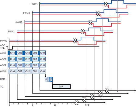
The TC179x high-end series features two GPTA modules and an additional LTCA block. This allows five complementary 3-phase PWM signals to be generated.
The start of the period is delayed in each case by the time of an ADC conversion process. The four ADC modules available in the TC1798 thus measure synchronously and – due to the time delay – in the middle of each period. Two ADC modules process the phase currents, whilst a further two modules can scan other signals simultaneously. With five 20 kHz 3-phase PWM signals, the CPU load remains under 10%.
Additional features
A further feature of the TriCore microcontroller, which should be used in frequency inverters, is the emergency stop mode that is implemented individually for each I/O port. To ensure that the outputs are reliably switched off in the event of an emergency, all the PWM signal outputs should for this reason be operated in emergency stop mode.
In case of an active emergency stop input signal, all the configured outputs are then set immediately to the required value, without software and without CPU clock; the power stage is reliably disconnected.
Thanks to its performance and its peripheral units, an AUDO MAX based frequency inverter can integrate additional PLC functionality. To this end, Infineon’s tool partners supply real-time operating systems and programming systems according to IEC61131-3.
It should be noted that further brushless DC motors in the case of the TC179x and TC172x derivatives can also be controlled by the capture compare unit (CCU6) known from the 16-bit microcontrollers.
The combination of RISC Harvard architecture with high-speed interrupt handling, hardware-assisted context switching, multiply accumulate (MAC) functionality and integrated FPU characterises the TriCore. The core has a superscalar design, which allows up to three processor commands to be executed at the same time.
It is thus possible, for example, for an algorithm to perform an arithmetic operation and load a data item from the memory at the same time. By using SIMD operations (single instruction multiple data), it is possible to parallelise and further accelerate data processing.
Following the first derivatives of the AUDO MAX family, the TC178x mid-range series, further innovations have been introduced. By way of example, to save system costs, the TC172x low-end series incorporates an internal voltage regulator in order to manage with just one supply voltage.
The TC179x high-end series features an enhanced processing kernel with a 6-stage pipeline to allow the CPU frequency to be increased to 300 MHz, whilst also offsetting the disadvantages of the higher response latency for a longer pipeline by means of improved branch prediction.
Further new features of the TC1.6 core in the TC179x relate to enhancements in division and multiplication operations and the floating-point arithmetic, which has now been integrated directly in the core and achieves up to two FLOPS per CPU clock. To achieve optimum processing power also when accessing the basically slower Flash, the AUDO-MAX family implements both a program cache and a data cache.
The AUDO MAX family extends the range of the safety features in order to satisfy functional safety requirements. As a result of using error correction code for SRAM and Flash, 1-bit errors in a word or double word are corrected without incurring access delays and 2-bit errors are detected, but not corrected.
A flexible CRC unit is available to the application developers for detecting errors in data packets. The memory protection unit (MPU), which restricts access to memory areas and, as such, permits absence of interaction of multiple tasks, has been supplemented in the case of the TC1.6 with a time protection mechanism, which helps to prevent run-time problems.
Another innovation comes in the form of the QFP ePad package (Figure 4) of the AUDO MAX family. An exposed pad of 8 x 8 mm with a thermal resistance of less than 1 K/W effectively supports heat dissipation.
The new TriCore AUDO MAX family (Figure 5) is suitable on account of its processing power and flexible GPTA timer unit both for sophisticated frequency inverters deployed in drive technology and for inverters used in wind turbines and solar inverters.

For more information contact Davis Moodley, Infineon, +27 (0)11 706 6099, www.infineon.com
| Email: | [email protected] |
| www: | www.infineon.com |
| Articles: | More information and articles about Infineon Technologies |


© Technews Publishing (Pty) Ltd | All Rights Reserved
 printer friendly version