
Current sensing is a fundamental requirement in virtually every item of equipment that features electronic control or supervision of its operation.
More sophisticated monitoring brings many benefits – longer battery life in handheld devices, more efficient and quieter operation of equipment that includes motors, and faster detection of fault conditions with benefits for safety, to list a few. Precision control depends on precision measurements, and accurate monitoring of current flow is an essential function.
This article discusses the fundamental concepts of current sensing resistors, current sensing techniques and outlines the advantages and disadvantages of three typical high-side sensing configurations.
Sense resistors
Current is almost always measured indirectly, often inferred from the voltage (V = IR) developed across a resistor placed in the current path. Current sense resistors are low-cost, can offer high measurement accuracy from very low to medium current levels, and are applicable to both AC and DC circuits.
Their disadvantages include adding an additional resistance into the measured circuit path, which may increase source output resistance and result in undesirable loading effect; and the associated power loss (P = I²R). Therefore, current sensing resistors are rarely used beyond low and medium current sensing applications. These disadvantages can be minimised by using low-value sensing resistors. However, the voltage drop across the sensing resistor may then become low enough to be comparable to the input offset voltage of subsequent analog conditioning circuitry, which would compromise measurement accuracy.
If the measured current has a significant high-frequency component, the sense resistor’s inherent inductance must be low, or the reactive voltage developed across it will degrade measurement accuracy. Other important parameters in the performance of a sense resistor include resistance tolerance, temperature coefficient, thermal EMF, temperature rating and power rating – which should be high enough to handle short duration and transient peaks.
Low- and high-side sensing
Two basic techniques can be categorised as low-side current sensing and high-side current sensing; each has advantages and disadvantages.
As shown in Figure 1, low-side current sensing connects the sensing resistor between the load and ground. Normally, the sensed voltage signal (VSEN = ISEN x RSEN) is so small that it needs to be amplified by subsequent op-amp circuits (eg, non-inverting amplifiers) to get the measurable output voltage (VOUT). This configuration provides low input common-mode voltage, with ground-referenced input and output, together with simplicity and low cost. But it is susceptible to ground path disturbance and the ground level seen by the load (application circuit) is lifted from system ground since RSEN adds undesirable resistance to the ground path. Other disadvantages are that any high load current caused by accidental short (to true ground) goes undetected; and the need for low VDD parts.
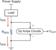
In a single-supply configuration, the most important aspect of low-side current sensing is that the common-mode input voltage range (VCM) of the op-amp must include ground. Low-side current sensing should be selected where short circuit detection is not required and ground disturbances can be tolerated.
As shown in Figure 2, high-side current sensing connects the sensing resistor between the power supply and load, eliminating ground disturbance effects, allowing the application to be directly connected to ground and enabling detection of short-circuit currents. However, the measurement arrangement must be able to handle very high and dynamic common-mode input voltages, leading to complexity and increased costs, and the need for high VDD parts.
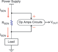
In a single-supply configuration, the VCM range of the difference amplifier must be wide enough to withstand high common-mode input voltages and the difference amplifier must be able to reject dynamic common-mode input voltages.
High-side sensing implementation
High-side current sensing is typically selected in applications where ground disturbance cannot be tolerated and short circuit detection is required, such as motor monitoring and control, over-current protection and supervising circuits, automotive safety systems and battery current monitoring.
Figure 3 shows the first of several high-side configurations; a single op-amp difference amplifier that consists of the MCP6H01 op-amp and four external resistors, to amplify the small voltage drop across the sensing resistor by the gain R2/R1, while rejecting the common-mode input voltage.
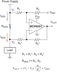
The difference amplifier’s common-mode rejection ratio (CMRRDIFF) is primarily determined by resistor mismatches (R1, R2, R1*, R2*), not by the op-amp’s CMRR; tight tolerance resistors will add cost. For R2/R1 = 1, resistor tolerances of 0,1% yield a worst case DC CMRRDIFF of 54 dB: if 1% resistors are used the figure will be only 34 dB (Reference 1 provides the detailed calculations).
RSEN should be much less than R1 and R2 in order to minimise resistive loading effects. The difference amplifier’s input impedances, seen from V1 and V2, are unbalanced. Note that the resistive loading effect and the unbalanced input impedances will degrade the CMRRDIFF.
The reference voltage (VREF) allows the amplifier’s output to be shifted to some higher voltage with respect to ground. VREF must be supplied by a low-impedance source, to avoid making CMRRDIFF worse. In addition, as shown in Figure 3, the input voltages (V1, V2) can be represented by common-mode input voltage (VCM) and difference-mode input voltage (VDM):
V1 = VCM + VDM/2 and V2 = VCM + VDM/2
VOUT = (V1 – V2) x G + VREF = VDM x G + VREF, where G = R2/R1
In order to prevent VOUT from saturating supply rails, it must be kept within the allowed VOUT range between VOL and VOH. The VCM range of the difference amplifier has been increased due to the resistor dividers made by R1, R2, R1* and R2*. In brief, this places limits on the difference amplifier’s VDM and VCM specifications; again, Reference 1 provides an example calculation.
In summary, difference amplifiers offer reasonable common-mode rejection ratio, wide common-mode input voltage range, low power consumption, low cost and simplicity. Their drawbacks include resistive loading effects, unbalanced input impedances and the fact that adjusting the difference amplifier’s gain requires changing more than one resistor value.
Three-op-amp instrumentation amplifier
Figure 4 shows the three-op-amp instrumentation amplifier (3-op-amp INA) that amplifies small differential voltages and rejects large common-mode voltages. Its first stage is a pair of high input impedance buffers (A1, A2) and resistors (RF and RG) that avoid both the input resistive loading effect and the unbalanced input impedances issue.
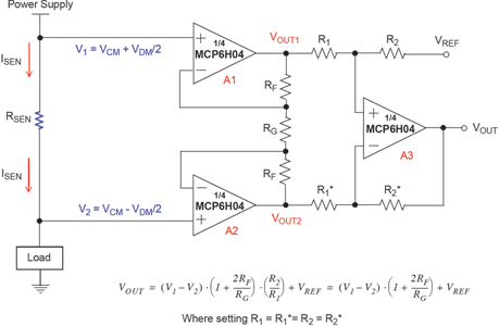
In addition, RF and RG increase the buffer pairs’ difference-mode voltage gains (GDM) to 1 + 2RF/RG while keeping their common-mode voltage gains (GCM) equal to 1. This significantly improves the 3-op-amp INA’s CMRR (CMRR3INA), as CMRR = 20 log (GDM/GCM). Another benefit is that the overall gain of the 3-op-amp INA can be modified by adjusting only the resistance of RG without having to adjust the values of R1, R1*, R2 and R2*.
The second stage is implemented by a difference amplifier (A3) which amplifies the difference-mode voltage and rejects the common-mode voltage. In a practical application, the R2/R1 ratio is usually set to 1. CMRR3INA is primarily determined by the difference-mode voltage gain of the first stage and net matching tolerance of R2/R1 and R2*/R1*. The tolerance of resistors RF and RG does not affect CMRR3INA.
For the 3-op-amp INA, there is a common issue that can be easily overlooked, ie, reduced common-mode input voltage range (VCM). Referring to Figure 4, the input voltages (V1, V2) can be represented by common-mode input voltage (VCM) and difference-mode input voltage (VDM). That is, V1 = VCM + VDM/2 and V2 = VCM - VDM/2.
The amplifiers (A1, A2) provide a difference-mode voltage gain (GDM) equal to the overall gain (G) and a common-mode gain (GCM) equal to 1. VOUT1, VOUT2 and VOUT must remain within the allowed output voltage range between VOL and VOH. The 3-op-amp INA configuration also places specific limits on VDM and VCM and, specifically, its VCM range will be significantly reduced when it operates in a high-gain configuration.
The 3-op-amp INA offers high common-mode rejection ratio (CMRR3INA), freedom from resistive loading effects, balanced input impedances and the ability to adjust the overall gain without needing to change more than one resistor value. Conversely, its VCM range is reduced and the increased number of op-amps increases power and cost.
Two-op-amp instrumentation amplifier
Compared to the 3-op-amp INA, the 2-op-amp INA in Figure 5 provides savings in cost and power consumption. Its input impedances are also very high, which avoids resistive loading effects and the unbalanced input impedances issue. Its common-mode rejection ratio (CMRR2INA) is primarily determined by the overall gain and the net matching tolerance of R2/R1 and R2*/R1*.
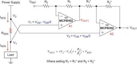
As shown in Figure 5, the input voltages (V1, V2) can be represented by common-mode input voltage (VCM) and difference-mode input voltage (VDM). That is, V1 = VCM – VDM/2, and V2 = VCM + VDM/2. Once again, VOUT and VOUT1 must stay in the allowed output voltage range between VOL and VOH, and this configuration also places limits on VDM and VCM values.
Unlike the 3-op-amp INA, the VCM range of the 2-op-amp INA will be significantly reduced when it operates in a low-gain configuration. Moreover, the circuit’s asymmetry in its common-mode signal path causes a phase delay between VOUT1 and V1, degrading the AC CMRR performance. Referring to Figure 5, the input signal V1 must pass through amplifier A1 before it can be subtracted from V2 by amplifier A2. Thus, the VOUT1 is slightly delayed and phase shifted with respect to V2. This is a significant limitation.
Figure 6 shows that by adding the resistor RG between two inverting inputs, the overall gain of the 2-op-amp INA can be easily set by adjusting only RG. The R2/R1 ratio is usually chosen for the desired minimum gain. Another benefit of adding the resistor RG is that the large resistor value usage of R2 and R2* can be avoided in very high-gain configurations. As with the other configurations, detailed calculations (Reference 1) yield the requirements for VDM and VCM, for the 2-op-amp INA with additional RG.
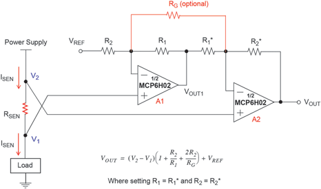
This final circuit arrangement offers high DC common-mode rejection (CMRR2INA), absence of resistive loading effect, balanced input impedances and reduced cost and power consumption, compared to the 3-op-amp INA. Its disadvantages include reduced VCM range, poor AC CMRR2INA due to the circuit’s asymmetry, and inability to operate at unity gain.
References
1. Zhen, Yang, ‘Current sensing circuit concepts and fundamentals’, Microchip Application Note AN1332.
2. Smither, M. A., Pugh, D.R. and Woolard, L.M., ‘C.M.R.R. analysis of the 3-op-amp instrumentation amplifier’, Electronics Letters, 2 Feb. 1989.
3. Sedra, A.S. and Smith, K.C., ‘Microelectronic Circuits’, 4th Edition, Oxford University Press, 1998.
| Email: | [email protected] |
| www: | |
| Articles: | More information and articles about Tempe Technologies |
© Technews Publishing (Pty) Ltd | All Rights Reserved