
Today, developments within the power conversion sector are driven by customer requirements for energy saving and physically smaller designs. Continual development of converter topologies for AC/DC and DC/DC has resulted in improved efficiency at the converter level.
Power MOSFETs are the core component of power converters in this market sector and are fundamental in producing an efficient design. Improvements in MOSFET designs allow circuit designers to utilise the improved device level performance, while increases in switching frequency and other critical parameters allow the converter design to operate more efficiently. In some cases, this may allow circuit design modifications that would not be possible without these improved MOSFET designs.
In 2006, the ‘OptiMOS 2’ 100 V MOSFET was introduced by Infineon in response to these requirements[1]. It was the first power MOSFET device within this voltage range that was based on charge compensation techniques. This resulted in a significant reduction of the MOSFET on-resistance over traditional designs, whilst retaining excellent switching behaviour.
The release of the OptiMOS 3 series improves the design further and allows higher-voltage devices to benefit from these technologies. OptiMOS 3 devices not only have ‘best in class’ performance in the 150 V to 250 V sector but combine this with several key parameters. The new devices exhibit low gate-charge characteristics, high switching speeds and good avalanche ruggedness. These attributes make them suitable for a wide variety of switch-mode power supply (SMPS) applications. These include high-efficiency AC/DC SMPS and DC/DC converters for telecommunication and server-based applications, Class-D amplifiers and motor control driver applications.
Device concept
The compensation principle for power MOSFETs was introduced in 1998 in commercially available products with the 600 V CoolMOS Technology[2]. The basic principle behind the drastic RDS(on) x A reduction compared to conventional power MOSFETs is the compensation of n-drift region donors by acceptors located in p-columns, as depicted in Figure 1.
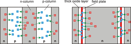
For lower breakdown voltages, trench field-plate MOSFETs are an excellent alternative. The application of a field-plate clearly improves the device’s performance. The device comprises a deep trench penetrating through most of the n-drift region. An insulated deep-source electrode, separated from the n-drift region by a thick oxide layer, acts as a field-plate and provides mobile charges required to balance the drift region donors under blocking conditions, as is shown schematically in Figure 1.
Standard MOS structures exhibit a linearly decreasing vertical electric field having maximum field strength at the body/drift region pn-junction. Such devices do not show a lateral component of the electric field. In a field-plate device, there is also a lateral component of the electric field and the space-charge region expands mainly in the lateral direction. Consequently, an almost constant vertical field distribution is achieved and the necessary drift-region length for a given breakdown voltage is significantly reduced. Simultaneously, the drift-region doping can be increased. Both techniques also result in a major reduction in on-state resistance.
Extending the device family towards higher blocking capability
The development of a new, space-saving and efficient edge-termination structure allows the OptiMOS 3 family to extend the benefits of this technology to devices up to 250 V[3].
The combination of the termination structure and charge compensation technologies results in exceptionally low RDS(on) and an excellent figure-of-merit (FOM = RDS(on) x QG). A comparison to the next best competitor device is given in Figure 2, clearly indicating the benefits of these technologies in terms of improved device performance. The culmination of these technological advances is a device that offers desirable solutions for a wide range of system requirements.
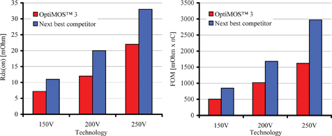
In high-current applications like motor control, lowest ohmic devices in D²-Pak and TO-220 minimise conduction losses and reduce the number of paralleled devices in the system. In fast switching applications, the very low gate-drain-charge QGD and FOMGD = RDS(on) x QGD cuts down on the switching losses and improves the overall efficiency. Devices available in SuperSO8 packages are therefore the ideal choice for applications like DC/DC converters or Class-D amplifiers. Furthermore, the very low on-resistance RDS(on) often allows for a package shrink: TO-247 packages can be replaced by TO-220 and a D²-Pak or TO-220 can often be replaced by a SuperSO8. The net result is a very compact solution which delivers excellent switching performance.
Another important issue is paralleling, especially in the case of high-current applications such as motor control. To meet the application requirements it is often advantageous to make use of complete power modules. This allows for improved heat management and lower parasitics, both boosting the overall performance. Here, the device count can be significantly reduced using the new device generation.
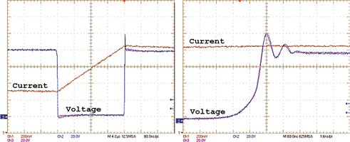
Figure 3 gives an example of the switching waveforms of large ‘OptiMOS 3’ 150 V chips paralleled in a power module. Here, a three-phase, full-bridge configuration was realised having eight chips in parallel on one DCB substrate with again two DCBs in parallel. Figure 3 shows the switching behaviour of one phase leg at a supply voltage of 80 V and a switched current of 500 A. The waveforms indicate a smooth switching behaviour with an acceptable overshoot voltage during the turn-off phase, with no problems being observed.
Choosing the right power package
With silicon technology moving rapidly forward, the package becomes an important factor for low-voltage MOSFETs. Especially the package inductance can play a major part in loss generation and in the overall device and application performance. Moreover, the on-resistance of the latest device technologies has become remarkably low, thus driving the need for low ohmic packages to avoid a limitation of the device by the package characteristics.
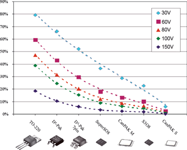
30 V technologies from most vendors today allow for MOSFET dies in a TO-220 with a lower on-resistance than the package resistance. The latest 60 V technologies on the market allow for devices with a package contribution of below 30% and even for 100 V technologies the package can already account for more than 20%, given a package resistance of 1 m. Therefore, the package resistance clearly limits the minimum on-resistance achievable. Additionally, a larger die is required for a given on-resistance, which also increases the gate charge and thus slows down the device switching.
Package contributions for devices with maximum die size for the most common low-voltage MOSFET classes are shown in Figure 4. To follow the route towards denser and more efficient power converter designs, new package types, such as the SuperSO8, S3O8 or the DirectFET/CanPAK, are needed to replace the leaded SMD or through-hole devices for low-voltage MOSFETs.
It is easily possible to estimate the losses due to package inductance for turn-off. As an example, a buck converter with an output current of 30 A, operating at 250 kHz, generates 0,7 W of losses in a D-Pak design due to the total package inductance of 6 nH. With a low inductive package like the SuperSO8, exhibiting an inductance of just 0,5 nH, the losses drop below 0,1 W. The lower package inductance also helps to avoid an unwanted turn-on of the MOSFET due to the source pin inductance in case of fast transients.
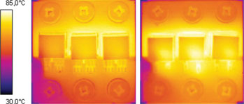
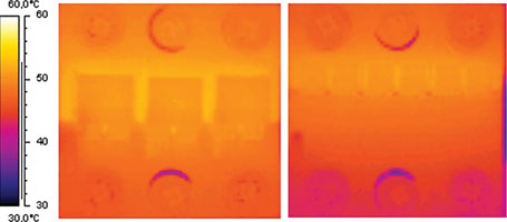
Another package-related topic is heat-spreading, which can be improved by either using an improved standard package or by completely shifting to newer package types. As shown in Figure 5, the use of a D²Pak with seven pins instead of a standard D²Pak already results in the avoidance of hot spots and a lower overall temperature. More advantages are gained if SuperSO8 packages are used. Figure 6 gives the comparison between D²Pak-7pin devices and the same amount of active silicon area packaged in SuperSO8 devices. Not only is the temperature behaviour improved and a smaller PCB area occupied, but the SuperSO8 packages also offer the chance to apply topside cooling for further improvements.
Summary
With the release of its OptiMOS 3 technology in the voltage classes 200 V and 250 V, Infineon Technologies now covers the full voltage range from 25 V to 250 V. With OptiMOS 3 being best-in-class for every single voltage class with respect to static and dynamic losses, customers are able to deliver future power converters with unprecedented efficiencies and power densities for a wide range of topologies.
References
[1] R. Siemieniec, F. Hirler, A. Schlögl, M. Rösch, N. Soufi-Amlashi, J. Ropohl and U. Hiller. A new and rugged 100 V power MOSFET, Proc. EPE-PEMC, 2006
[2] G. Deboy, M. Mürz, J.-P. Stengl, H. Strack, J. Tihanyi and H. Weber. A new generation of high voltage MOSFETs breaks the limit line of silicon, Proc. IEDM, 683-685, 1998
[3] R. Siemieniec, F. Hirler and C. Geissler. Space-saving edge-termination structures for vertical charge compensation devices, Proc. EPE, 2009
For more information contact Davis Moodley, Infineon, +27 (0)11 706 6099, www.infineon.com
| Email: | [email protected] |
| www: | www.infineon.com |
| Articles: | More information and articles about Infineon Technologies |
© Technews Publishing (Pty) Ltd | All Rights Reserved