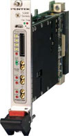

Pentek’s Model 5342 is a multichannel, high-speed data converter suitable for connection to HF or IF ports of a communications system. It includes four A/Ds with one up-converter and D/A converter. The board features built-in support for PCI Express (PCIe) Gen 2 over the 3U VPX backplane. A fabric-transparent crossbar switch configuration adds Gigabit serial data paths for Xilinx Aurora or Serial RapidIO applications.
The front end accepts four full-scale analog HF or IF inputs on front panel MMCX connectors at +10 dBm into 50 Ω with transformer coupling into 14-bit, 125 MHz A/Ds. The digital outputs are delivered into a Virtex-4 FPGA for signal processing or for routing to other module resources. The 5342 features a TI DAC5686 digital up-converter (DUC) and D/A. It accepts a baseband real or complex data stream from its FPGA with signal bandwidths up to 40 MHz.
When operating as an up-converter, the DAC5686 interpolates and translates real or complex baseband input signals to any IF centre frequency between DC and 160 MHz. It delivers real or quadrature (I+Q) analog outputs up to 320 MHz to the 16-bit D/A converter. If translation is disabled, the DAC5686 acts as an interpolating 16-bit D/A with output sampling rates up to 500 MHz.
The board’s architecture includes two Virtex-4 FPGAs. All of the board’s data and control paths are accessible by the FPGAs, enabling factory installed functions including data multiplexing, channel selection, data packing, gating, triggering and SDRAM memory control. In addition, users can include their own custom IP, and integrate it with factory-shipped functions using a Pentek GateFlow FPGA design kit.
The Xilinx XC4VSX55 FPGA serves as a control and status engine with data and programming interfaces to each of the onboard resources including the A/D converters, DDR2 SDRAM memory, digital up-converter and D/A converter. The XC4VSX55 features 512 DSP slices and is ideal for implementing functions such as demodulation/modulation, digital delay and channelisation. For applications requiring more FPGA logic cells, the Model 5342 can be optionally configured with an XC4VLX100 for up to 221 184 logic cells.
A Virtex-4 XC4VFX60 interface FPGA provides board interfaces including PCI and serial I/O. The interface FPGA also includes two PowerPC cores which can be used as local microcontrollers to create complete application engines. The Model 5342 can be optionally configured with XC4VFX100 in place of each FX60. Another option provides general purpose I/O to VPX-P2 with 16 pairs of LVDS connections to the processing FPGA, and 16 pairs of LVDS connections to the interface FPGA for custom I/O.
A front-panel, 26-pin LVDS clock/sync connector allows multiple modules to be synchronised. In slave mode, each accepts differential LVDS inputs that drive the clock, sync and gate signals for the two internal timing buses. In master mode, each LVDS bus can drive one or both sets of timing signals from the two internal timing buses for synchronising multiple modules. Up to seven slave 5342s can be driven from the LVDS bus master, supporting synchronous sampling and sync functions across all connected modules.
Three independent 256 MB banks of DDR2 SDRAM are available to the SX55 or LX100 FPGA. Built-in memory functions include an A/D data transient capture mode with pre- and post-triggering and a D/A waveform generator mode. All memory banks can be accessed through the PCI interface using the onboard DMA controllers.
| Tel: | +27 21 975 8894 |
| Email: | [email protected] |
| www: | www.ri-tech.co.za |
| Articles: | More information and articles about Rugged Interconnect Technologies |
© Technews Publishing (Pty) Ltd | All Rights Reserved