
There are three driving forces that are radically changing CAD library construction. The first is lead-free solder. The next is metric units. And lastly is ‘component manufacturer chaos’. This term describes component manufacturers who no longer follow JEDEC packaging standards and are leading the way for new component package development.
It seems as though the constraints of standard package data have been thrown out the window and new unique electronic device packages are emerging on the market at lightning speed. These challenges will continue to impact CAD library development and maintenance as we move forward.
Solder
Using lead solder allows the CAD designer to create land patterns that accommodate a variety of alternate component packages that have slightly different component lead dimensions. The land pattern pads can have various toe, heel and side fillets and due to the wetting (flow) of the lead solder, it will compensate for the inaccuracy of the land pattern up to a certain point. However, when using lead-free solder, the land pattern size and pad spacing should be as accurate as possible and only a good land pattern calculator or a good mathematician can determine the best lead-free solder joint goals for each unique component.
J-lead and gull wing component leads are good for lead solder, but they are not optimal component leads for lead-free technology due to low wetting of lead-free solder. Component manufacturers are producing new lead forms that are more compatible with the lead-free solder process. These new component leads are referred to as ‘no-lead’ packages and come in a variety of package styles, as shown in Figure 1.
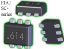
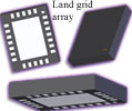
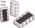
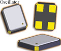
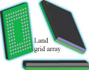
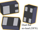
The ‘flat no-lead’ land pattern does not have the typical ‘toe, heel and side’ solder joint goal as the popular J-lead and gull wing packages; rather flat no-lead requires a ‘periphery’ land area which has the same shape as the component lead, just slightly larger for paste mask disbursement.
The flat no-lead requires a very accurate land pattern with tight tolerances. The flat no-lead gets 100% covered with paste mask and the overflow solder runs out to the land pattern pad edge when the PCB runs through the reflow oven. Because the component leads are underneath the flat no-lead package it has a significant packaging density advantage. As an example, the current chip resistor and capacitor has a wraparound component lead. Great caution must be taken because the J-STD-001D assembly standard allows for chip component overhang of up to 50% of the component width for Class 1 and Class 2 and 25% for Class 3 (the A dimension in Figure 2). Figure 2 shows the typical chip component that could cause short circuiting of the wrap around component leads.
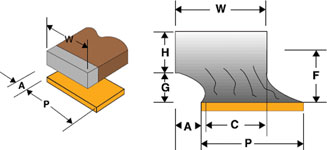
If two chip components are placed too close side by side, there is a risk of a short circuit. However, the 2-pin DFN package has the component leads under the component body and recessed inward away from the component body edge. The plastic body of the DFN component can touch and there is no risk of short circuiting. The same principle is true for all flat no-lead component packages with pullback leads.
Metric units
The EU Council Directive 80/181/EEC requires use of the metric measurement system. Beginning 1 January 2010, the European Union (EU) Council Directive 80/181/EEC (Metric Directive) will allow the use of only metric units, and prohibit the use of any other measurements for most products sold in the EU. This will make the sole use of metric units obligatory in all aspects of life in the EU.
This will have a profound effect on the electronics industry worldwide. All world standards organisations have already adopted the metric measurement system and that is the only dimensional data that they are providing INEMI and component manufacturers. Many of today’s component datasheets only provide metric dimensions and Imperial units are starting to slowly fade away. This makes the process of building CAD library parts using Imperial units intolerable. Most companies worldwide have resorted to building all CAD libraries using metric dimensions, but many companies have still not converted to the metric system for PCB layout, which further complicates productivity.
Even though the USA is the only industrialised nation that has not adopted the metric measurement system as the preferred system, every country in the world uses the Imperial measurement system for PCB layout. This is primarily due to several factors:
* Component dimensions in the 1980s were predominately Imperial units.
* CAD vendor default values are in Imperial units.
* PCB manufacturers prefer Imperial units due to the material manufacturer’s delivering in Imperial units.
* Assembly shops do not care one way or the other, but refer to component package data in Imperial units, such as a capacitor or resistor package 1206 = 0,125” x 0,062” when in reality the package dimensions are 3,2 mm x 1,6 mm = 3216, but assembly shops do not refer to a 1206 as 3216.
The eventual goal of all world standards is for CAD librarians to build all their library parts using the metric unit system. This goal will eventually spill over to the PCB layout where parts placement and trace routing will be performed using metric units. The only major roadblock in making the full transition to metric units is that PCB fabrication material manufacturers need to convert to metric units. Once this happens, the entire PCB industry will transition, since PCB manufacturers will prefer metric-based PCB layouts because it will allow them to work with a single measurement system.
Component manufacturer chaos
World standards are taking a big hit in this area as they cannot keep up with fast paced component package development for high-speed design and lead-free packaging. Also, corporate greed has crept into the electronics market, setting off global competition for electronic devices.
The reality is simple. It is in the best interest for every component manufacturer to be competitive for survival. This means that developing unique component packages that are smaller, cheaper, lead-free, high-speed, low-profile and hermetically sealed is the current trend. Following existing JEDEC packaging standards is out and developing unique component packages is in. It is in the best interest for the component manufacturer’s stockholders, employees, CEO and CFO to create unique component packages that require a unique CAD library part to eliminate as much competition as possible – cornering the market with their unique component package to generate the highest profit margin.
This phenomenon is taking its toll on CAD librarians trying to keep pace with the increasing number of unique packages. It is also wreaking havoc on world standards as they are forced to take a back seat and watch and have no say on what component manufacturers are producing. As an end result, the CAD library at every electronics based company is growing at an unprecedented rate.
Unfortunately, many component manufacturers have stopped providing recommended land patterns and the need for new software tools that automatically calculate CAD land pattern technology is rapidly growing. The IPC-7351A land pattern standard is having a very difficult time keeping pace with new component package technology, particularly in the land pattern naming convention.
Examples of what component manufacturers are currently doing to make their device packages unique include:
* Making two-pin devices with Pin 1 a different size than pin 2 or vice versa.
* Making thermal tabs under parts various unique sizes.
* Reverse order pin assignments.
* Randomly deleting or hiding (skip over) pins.
* Inventing new component lead forms.
* Introducing unique pin pitch packages.
* Bending and trimming component leads at various lengths and sizes.
* Component lead tolerances vary from one manufacturer to another.
Every one of these items requires the creation of unique CAD library parts. This is also the reason why trying to create world standards is difficult. There is no end in sight to what component manufacturers are going to introduce next. It is almost a case of 'Surprise! Here is the latest CPU processor from Intel' and it is a complex, high pin count BGA with pins placed on a staggered and random grid that no standard committee would ever approve and there are no CAD tools that can easily build these library parts. The new complex high pin count BGA CAD library parts take 2–3 hours to manually build. There are industry guesstimates that there are over 2 million man hours of duplicated effort spent every year by PCB designers and CAD librarians building the same exact CAD library part. That is equivalent to 1000 full time jobs of duplication of effort and this is probably an underestimate.
CAD library solutions
Anyone who aspires to build massive CAD libraries for the purpose of eliminating duplication is chasing a dream. With so many new component families that are being introduced and new innovative electronic devices being invented, as soon as one thinks they are done, half of what they produced is obsolete and hundreds of new component packages become available every week. Thousands of new unique component packages are introduced every year and just as many are going to be obsolete every year.
Electronics companies use about 20% of the same component packages; the other 80% of the component devices are unique for each company. Managing a CAD library then becomes a task unique to each corporation because no two companies use the same electronic components and therefore have to manage their own unique CAD library.
The concept for companies that sell canned libraries to the public is changing from a product to a service that will build parts on demand. Also, software companies who offer an average starter library and software tools that automate CAD library construction (like the IPC-7351A LP Calculator and CAD interface) are becoming the new solution for creating and maintaining CAD libraries. The reality of purchasing a CAD library that contains 10000 parts is that the customer will only actually use 500–1000 of those parts and never use the other 9000 parts that they purchased. Besides, the customer will still be required to create 20%–30% of the CAD library parts that they need because many parts did not come with the CAD library they purchased.
Purchasing software tools that automate CAD library construction is the best alternative to quickly build accurate parts. The tool should also store the component and land pattern data into a file that can be used for historical library documentation. This file should contain everything one needs to regenerate a CAD library in any CAD format that one wishes to use.
This eliminates duplication of effort when changing CAD tools. The library documentation should be customised to only the parts that the customer uses. Their library documentation should never change or never need to be recreated if they change CAD tools. Library documentation should be generic to all CAD tools. Also, if a user ever has a need to change any rule or feature in their CAD library, they need a tool that can globally update their entire library with a single mouse click.
Building and managing CAD libraries is not getting easier, but there are free products available, such as Mentor Graphics’ IPC-7351B LP Viewer.
| Tel: | +27 11 315 8316 |
| Email: | [email protected] |
| www: | www.asic.co.za |
| Articles: | More information and articles about ASIC Design Services |

© Technews Publishing (Pty) Ltd | All Rights Reserved