


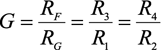
PIN diodes, which sandwich a lightly doped intrinsic (I) region between heavily doped P and N regions, are used extensively in RF and microwave applications. Common applications of PIN diodes are microwave switches, phase shifters and attenuators, where high isolation and low loss are required.
They can be found in test equipment, instrumentation, communications gear, radar and a variety of military applications.
Every PIN diode in a switching circuit has an accompanying PIN diode driver or switch driver that provides a controlled forward bias current, a reverse bias voltage, and the activating interface between the control signal – typically a digital logic command – and one or more PIN diodes. This driver function can be rendered as a discrete design, or with specialised ICs to fit the application.
As an alternative, widely available op-amps and specialty amplifiers, such as clamp amplifiers and differential amplifiers, can be used in place of discrete PIN-diode drive circuits and expensive PIN-diode driver ICs. Op-amps in this class feature wide bandwidth, high slew rates and more than enough steady-state current to drive PIN diodes. This article discusses three different PIN-driver circuits that employ op-amps or specialty amplifiers – the AD8037, AD8137 and ADA4858-3. The circuits are designed to work with single-pole double-throw (SPDT) PIN-diode switches, but they can be adapted for other circuit configurations as well.
PIN diodes
PIN diodes are used as current-controlled resistors at RF and microwave frequencies, with resistances that can range from a fraction of an ohm when forward biased, or on, to greater than 10 kΩ when reverse biased, or off. Differing from typical PN junction diodes, PIN diodes have an additional layer of highly resistive intrinsic semiconductor material (the I in PIN) sandwiched between the P and N material (Figure 1).

When a PIN diode is forward biased, holes from the P material and electrons from the N material are injected into the I region. The charges cannot recombine instantaneously; the finite amount of time required for them to recombine is called the carrier lifetime. This causes a net stored charge in the I region, reducing its resistance to a value designated as RS, the effective on-resistance of the diode (Figure 2a).
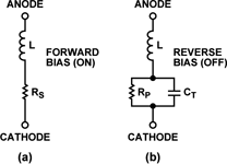
When a reverse- or zero-bias voltage is applied, the diode appears as a large resistance, RP, shunted by a capacitance, CT (Figure 2b). By varying the diode geometry, it is possible to tailor PIN diodes to have a variety of combinations of RS and CT to meet the needs of various circuit applications and frequency ranges.
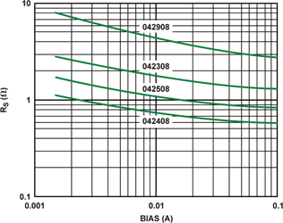
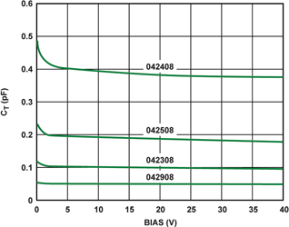
The combination of steady-state bias current, ISS, and reverse voltage provided by the driver determines the final values of RS and CT. A set of relationships for members of a typical family of PIN diodes can be seen in Figure 3 and Figure 4 – for M/A-COM MADP 042XX8-13060(1) series silicon diodes. The diode material affects its properties. For example, gallium-arsenide (GaAs) diodes require little – if any – reverse bias to achieve a low value of CT, as shown in Figure 9.
The stored charge in a PIN diode can be approximated by Equation 1.
where:
QS = stored charge
tau = diode carrier lifetime
ISS = steady-state current
To turn the diode on or off, the stored charge must be injected or removed. The driver’s job is to inject or remove this stored charge very quickly. In cases where the switching time is less than the carrier lifetime of the diode, the peak current (IP) required to effect fast switching can be approximated by Equation 2.

where:
t = required switching time
ISS = the steady-state current provided by the driver that sets the PIN-diode on-resistance, RS
tau = carrier lifetime
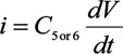
The driver injection or removal current, or spiking current, i, can be expressed by Equation 3.

where:
C = capacitance of the driver output capacitors, or spiking caps
v = voltage across the output capacitors
dv/dt = time rate of change of voltage across the capacitors
PIN-diode bias interface
Connecting the switch driver control circuit to a PIN diode such that it can turn diodes on and off by applying a forward or reverse bias is a challenging task. The bias circuit typically uses a low-pass filter between the RF circuit and the switch driver. Figure 5 shows a single-pole double-throw (SPDT) RF switch and its bias circuit. When properly implemented, filters L1/C2 and L3/C4 allow control signals to be applied to PIN diodes D1–D4 with minimal interaction with the RF signal – which is switched from RF IN to PORT 1 or PORT 2.
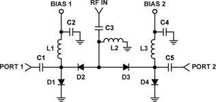
These elements allow the relatively lower frequency control signals to pass through to the PIN diodes but keep the high-frequency signal from escaping the RF signal path. Errant RF energy loss means undesirably higher insertion loss for the switch. Capacitors C1, C3 and C5 block the DC bias that is applied to the diodes from invading the circuitry in the RF signal path. Inductor L2, in the DC return path to ground, lets DC and low-frequency switch-driver signals pass with ease but presents a high impedance at RF and microwave frequencies, reducing RF signal loss.
Because the bias-, RF- and switch-driver circuits all interact and affect each other’s performance, trade-offs are essential, as in any design. For example, if C2 and C4 are large (>20 pF) – desirable for RF performance – the driver has a problem because large capacitances result in slower rising and falling edges. Fast switching is desired in most applications, so the capacitances must be kept to a minimum for optimum driver performance, yet be high enough to meet the RF circuit requirements.
Traditional PIN-diode drivers
PIN-diode drivers come in a variety of shapes and sizes. Figure 6 is a schematic of a typical discrete switch driver that provides good switching speed. Such drivers can be realised with either chip-and-wire (hybrid) construction, which is very expensive, or with surface-mount components, which are inexpensive but require more printed circuit board area than a hybrid.

Dedicated switch-driver integrated circuits are also available; they are compact, provide a TTL interface, and have good performance, but their flexibility is limited and they tend to be expensive. Another kind of switch-driver architecture that should be considered employs operational amplifiers. A clear advantage of op-amp switch drivers is their inherent flexibility. They can be easily configured for a variety of applications, supply voltages and conditions to provide the designer with a multitude of design options.
Op-amp PIN-diode drivers
Op-amp circuits are an attractive alternative to traditional PIN-diode drivers. Besides being flexible, they can operate with transition speeds often approaching or exceeding 1000 V/μs. Three different amplifier circuits for driving RF PIN diodes will be shown here. The amplifiers chosen are intrinsically different, yet they all perform a similar function. These amplifier circuits will drive silicon- or gallium-arsenide (GaAs) PIN diodes, but each has something different to offer.
AD8037 – a clamp amplifier
This circuit can operate up to 10 MHz with excellent switching performance and a total propagation delay of 15 ns. The output voltage and current can be tweaked to fit different applications by varying either the gain or the clamp voltages. The AD8037(2) clamp amplifier, originally designed to drive ADCs, provides a clamped output to protect against overdriving the ADC input. In the configuration of Figure 7, a pair of AD8037s (U2 and U3) are used to drive PIN diodes.

Here U2 and U3 are set for a non-inverting gain of 4. The AD8037’s unique input clamp feature allows extremely clean and accurate clamping. It amplifies the input signal linearly up to the point where the gain, multiplied by the positive and negative clamp voltages (VCH and VCL), is exceeded. With a gain of 4 and clamp voltages of ±0,75 V, the output voltage will be four times the input voltage for inputs smaller than ±0,75 V but will be clamped to a maximum of ±3 V when the input signal is larger than ±0,75 V.
This clamping feature allows for very fast recovery (typically less than 2 ns) from overdrive. The clamp voltages (VCH and VCL) are derived by voltage dividers R2, R3, R7 and R8. The digital interface is implemented by a 74F86 XOR logic gate (U1), which provides drive signals for U2 and U3 with minimal propagation-delay skew between the two complementary outputs.
The network of resistors – R4, R5, R6 and R9 – provides level shifting of the TTL outputs to approximately ±1,2 V, which is fed to U2 and U3 via R10 and R12. The ±1,2 V inputs to U2 and U3 provide 60% overdrive, ensuring that the outputs will go into the clamped state (4 x 0,75 V). Thus, the output levels for the silicon PIN-diode driver are set to ±3 V. Resistors R16 and R17 limit the steady-state current. Capacitors C12 and C13 set the spiking current for the PIN diodes.
AD8137 – a differential amplifier
Differential amplifiers, such as the AD8137 used in this example, provide exceptional high-speed switching performance at low cost and offer the designer great flexibility in driving various types of RF loads. A variety of differential amplifiers(3) are available, including faster and higher-performance devices.
The AD8137(4) high-speed differential amplifier, typically used for driving ADCs, can also serve as a low-cost, low-power PIN diode driver. Achieving typical switching times of 7 ns to 11 ns, including the propagation delays of the driver and the RF load, it features complementary outputs and is a versatile alternative to more expensive conventional drivers.
The circuit of Figure 8 converts a single-ended TTL input (0 V to 3,5 V) to a complementary ±3,5 V signal, while minimising propagation delay. The TTL signal is amplified by a factor of 4 to produce the required ±3,5 V swing at the AD8137 outputs. The midpoint (or common-mode voltage) of the TTL signal is 1,75 V; the same value must be applied to R2, as VREF, to avoid introducing a common-mode offset error at the amplifier outputs. It is best to drive this point from a low source impedance; any series impedance will add to R1 and affect the amplifier gain.

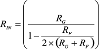
The output voltage gain is established by Equation 4.
To properly terminate the pulse generator input impedance into 50 Ω, the input impedance of the differential amplifier circuit needs to be determined. This can be calculated using Equation 5, which gives RT = 51,55 Ω, for which the closest standard 1% value is 51,1 Ω. For a symmetrical output swing it is important that the two input networks have the same impedance. This means that the inverting input impedance must incorporate the Thévenin impedance of the source and termination resistance into the gain-setting resistance, R2. For a more detailed explanation see Application Note AN-1026.(3)
In Figure 8, R2 is roughly 20 Ω larger than R1 to compensate for the additional resistance (25 Ω) introduced by the parallel combination of the source resistor, RS, and termination resistor, RT. Setting R4 to 1,02 kΩ, the closest standard value to 1,025 kΩ, ensures that the two resistor ratios are equal, to avoid introducing a common-mode error.
Output level shifting is easily accomplished using the AD8137’s VOCM pin, which sets the DC output common-mode level. In this case the VOCM pin is tied to ground for a symmetrical output swing around ground.
Resistors R5 and R6 set the steady-state PIN-diode current as shown in Equation 6.

Capacitors C5 and C6 set the spiking current, which helps inject and remove the stored charge in the PIN diodes. Their capacitance values can be adjusted to optimise the performance required for a particular diode load. The spiking current can be determined by Equation 7.
ADA4858-3 – a triple op-amp with charge pump
Many applications make available just a single supply. This can often be problematic for the circuit designer, especially when looking for low off-capacitance in PIN circuits. In such cases an op-amp that has an onboard charge pump is useful in a circuit to drive silicon or GaAs PIN diodes without requiring an external negative supply. This can provide significant savings by conserving space, power and budget.
One such device is the ADA4858-3,(6) a high-speed, current-feedback triple amplifier with the distinguishing feature that it includes an onboard charge pump that enables the output to swing –3 V to –1,8 V below ground, depending on the supply voltage and loading. It is robust enough to actually power other circuitry with up to 50 mA of negative supply current.
The ADA4858-3 provides a unique solution to the problem of driving a complementary PIN-diode microwave switch in a single-supply system. Recalling Figure 4, it can be seen that, depending on the PIN diode type, even a small amount of reverse bias helps lower the diode capacitance, CT. GaAs PIN diodes benefit from this type of driver, as they typically do not require as much negative bias to keep their off-capacitance (CT) low (Figure 9).
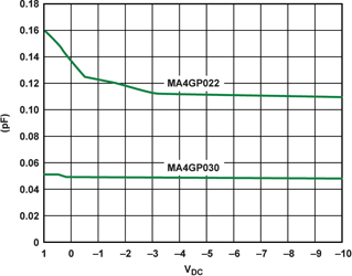
Figure 10 shows a circuit using the ADA4858-3 as a PIN-diode driver. A buffer gate can be added to the input to make the circuit compatible with TTL or other logic. For this circuit, the requirement is to convert a TTL 0 V to 3,5 V input signal swing to a complementary –1,5 V to +3,5 V swing for driving PIN diodes.
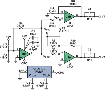
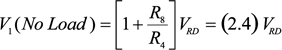
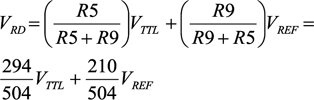
R1, R2, R3 and U1C form a –1,5 V reference for the circuit with the internal negative voltage, CPO, generated by the on-chip charge pump. Capacitors C3 and C4 are required for charge pump operation. The negative reference is then summed passively with the VTTL input via voltage divider (R5 and R9). The resulting voltage (VRD) appears at the non-inverting input of U1B. The U1B output voltage can be calculated using Equation 8.
where:
The negative reference is also fed to amplifier U1A where it is summed with the TTL input; the resulting output voltage, V2, can be calculated using Equation 10.
Since these amplifiers employ a current-feedback architecture, attention must be paid to the choice of feedback resistance, which plays a major role in the stability and frequency response of the amplifier. For this application, the feedback resistor is set at 294 Ω, as recommended in the data sheet.
Output voltages V1 and V2 can be described by Equation 8 and Equation 10, respectively. The amount of output spiking current can be determined using Equation 3 for the voltage across capacitors C5 and C6. The steady-state current, which sets the PIN diode on-resistance, is established by voltage differences across R11 and R12 and depends on the PIN diode curves and system requirements.
For this application, the RF switch load was a MASW210B-1 silicon PIN diode SPDT switch, used in the front end of a microwave down-converter (Figure 11).

The switch output waveform and the TTL input signal are shown in Figure 12. Note the fast rising and falling edges. This application did not use spiking caps, C5 and C6, due to the relatively slow switching time requirement of the switch, approximately 50 ns. R11 and R12, which establish the steady-state diode current, were 330 Ω resistors.
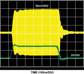
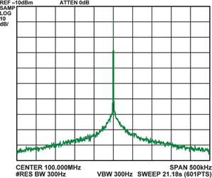
Figure 13 shows the spectral frequency response of the down-converter front end with switch SW1 in a fixed position to check insertion loss. Note the absence of harmonics or sidebands – a good indication that there are no perceptible 100 kHz switching artefacts emanating from the ADA4858-3’s on-chip charge pump – an important consideration when using these devices in this type of application.
Conclusion
As these three examples show, op-amps can provide creative alternatives to traditional drivers, with performance rivalling that of dedicated ICs designed solely for driving PIN diodes. Furthermore, op-amps afford the ability to tailor gains, manipulate inputs and – when using devices containing an internal charge pump – eliminate a negative supply, adding a dimension of flexibility to the design of drivers for PIN diodes and other circuitry. Easy to use and configure, op-amps solve complex problems with relative ease.
Acknowledgements
The switching-speed and spectral data, RF load and test equipment were provided courtesy of Sage Laboratories, Hudson, NH. The tests were facilitated by Tony Cappello, CTO, with technical assistance provided by David Duncan, VP of Engineering.
References
Hiller, Gerald. Design with PIN Diodes.
M/A-COM Application Note AG312.
Understanding RF/Microwave Solid State Switches and Their Applications. Agilent Application Note.
1. www.macomtech.com/datasheets/MADP-042008_Series.pdf
5. www.analog.com/static/imported-files/application_notes/ AN-1026.pdf
6. www.analog.com/en/audiovideoproducts/video-ampsbuffersfilters/ada4858-3/products/product.html


© Technews Publishing (Pty) Ltd | All Rights Reserved
 printer friendly version