


Metastability is a phenomenon that can cause system failure in digital devices, including FPGAs, when a signal is transferred between circuitry in unrelated or asynchronous clock domains.
This article describes metastability in FPGAs, explains why the phenomenon occurs, and discusses how it can cause design failures.
The calculated mean time between failures (MTBF) due to metastability indicates whether designers should take steps to reduce the chance of such failures. This article explains how MTBF is calculated from various design and device parameters, and how both FPGA vendors and designers can increase the MTBF. System reliability can be improved by reducing the chance of metastability failures with design techniques and optimisations.
What is metastability?
All registers in digital devices such as FPGAs have defined signal timing requirements that allow each register to correctly capture data at its inputs and produce an output signal. To ensure reliable operation, the input to a register must be stable for a minimum time before the clock edge (register setup time or tSU) and for a minimum time after the clock edge (register hold time or tH). The register output is then available after a specified clock-to-output delay (tCO).
If a data signal transition violates a register’s tSU or tH requirements, the output of the register may go into a metastable state. In a metastable state, the register output hovers at a value between the high and low states for some period of time, which means the output transition to a defined high or low state is delayed beyond the specified tCO.
In synchronous systems, the input signals must always meet the register timing requirements, so metastability does not occur. Metastability problems commonly occur when a signal is transferred between circuitry in unrelated or asynchronous clock domains. The designer cannot guarantee that the signal will meet tSU and tH requirements in this case, because the signal can arrive at any time relative to the destination clock.
However, not every signal transition that violates a register’s tSU or tH results in a metastable output. The likelihood that a register enters a metastable state and the time required to return to a stable state vary depending on the process technology used to manufacture the device and on the operating conditions. In most cases, registers will quickly return to a stable defined state.
A register sampling a data signal at a clock edge can be visualised as a ball being dropped onto a hill, as shown in Figure 1. The sides of the hill represent stable states – the signal’s old and new data values after a signal transition – and the top of the hill represents a metastable state. If the ball is dropped at the top of the hill, it might balance there indefinitely, but in practice it falls slightly to one side of the top and rolls down the hill. The further the ball lands from the top of the hill, the faster it reaches a stable state at the bottom.
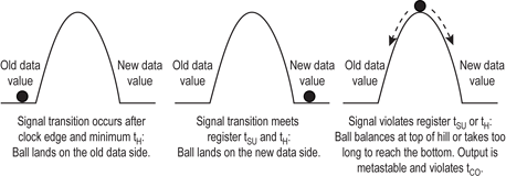
If a data signal transitions after the clock edge and the minimum tH, it is analogous to the ball being dropped on the 'old data value' side of the hill, and the output signal remains at the original value for that clock transition. When a register’s data input transitions before the clock edge and minimum tSU, and is held beyond the minimum tH, it is analogous to the ball being dropped on the 'new data value' side of the hill, and the output reaches the stable new state quickly enough to meet the defined tCO time. However, when a register’s data input violates the tSU or tH, it is analogous to the ball being dropped on the hill. If the ball lands near the top of the hill, the ball takes too long to reach the bottom, which increases the delay from the clock transition to a stable output beyond the defined tCO.
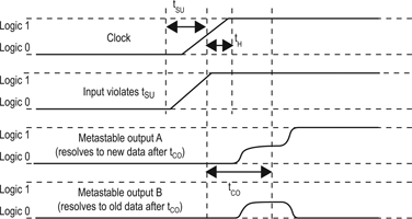
Figure 2 illustrates metastable signals. The input signal transitions from a low state to a high state while the clock signal transitions, violating a register’s tSU requirement. The data output signal examples start in the low state and go metastable, hovering between the high and low states. The signal output A resolves to the input data’s new logic 1 state, and output B returns to the data input’s original logic 0 state. In both cases, the output transition to a defined 1 or 0 state is delayed beyond the register’s specified tCO.
When does metastability cause design failures?
If the data output signal resolves to a valid state before the next register captures the data, then the metastable signal does not negatively impact the system operation. But if the metastable signal does not resolve to a low or high state before it reaches the next design register, it can cause the system to fail.
Continuing the ball and hill analogy, failure can occur when the time it takes for the ball to reach the bottom of the hill (a stable logic value 0 or 1) exceeds the allotted time, which is the register’s tCO plus any timing slack in the path from the register. When a metastable signal does not resolve in the allotted time, a logic failure can result if the destination logic observes inconsistent logic states, that is, different destination registers capture different values for the metastable signal.
Synchronisation registers
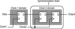
When a signal transfers between circuitry in unrelated or asynchronous clock domains, it is necessary to synchronise this signal to the new clock domain before it can be used. The first register in the new clock domain acts as a synchronisation register.
To minimise the failures due to metastability in asynchronous signal transfers, circuit designers typically use a sequence of registers (a synchronisation register chain or synchroniser) in the destination clock domain to resynchronise the signal to the new clock domain. These registers allow additional time for a potentially metastable signal to resolve to a known value before the signal is used in the rest of the design. The timing slack available in the synchroniser register-to-register paths is the time available for a metastable signal to settle, and is known as the available metastability settling time.
A synchronisation register chain, or synchroniser, is defined as a sequence of registers that meets the following requirements:
* The registers in the chain are all clocked by the same or phase-related clocks.
* The first register in the chain is driven from an unrelated clock domain, or asynchronously.
* Each register fans out to only one register, except the last register in the chain.
The length of the synchronisation register chain is the number of registers in the synchronising clock domain that meet the above requirements. Figure 3 shows a sample synchronisation chain of length two, assuming the output signal feeds more than one register destination.
Note that any asynchronous input signals, or signals that transfer between unrelated clock domains, can transition at any point relative to the clock edge of the capturing register. Therefore the designer cannot predict the sequence of a signal’s transitions or the number of destination clock edges until the data transitions. For example, if a bus of asynchronous signals is transferred between clock domains and synchronised, the data signals could transition on different clock edges. As a result, the received values of the bus data could be incorrect.
The designer must accommodate this behaviour with circuitry such as dual-clock FIFO (DCFIFO) logic to store the signal values, or hand-shaking logic. FIFO logic uses synchronisers to transmit control signals between the two clock domains, and then data is written and read with dual-port memory. Altera offers a DCFIFO megafunction for this operation, which includes various levels of latency and metastability protection for the control signals. Otherwise, if an asynchronous signal acts as part of hand-shaking logic between two clock domains, control signals indicate when data can be transferred between clock domains. In this case, synchronisation registers are used to ensure that metastability will not interfere with the reception of control signals and that the data has enough settling time for any metastable conditions to resolve before the data is used. In a properly designed system, the design functions correctly as long as each signal resolves to a stable value before it is used.
Calculating metastability MTBF
The mean time between failures, or MTBF, due to metastability provides an estimate of the average time between instances when metastability could cause a design failure. A higher MTBF (such as hundreds or thousands of years between metastability failures) indicates a more robust design. The required MTBF depends on the system application. For example, a life-critical medical device requires a higher MTBF than a consumer video display device. Increasing the metastability MTBF reduces the chance that signal transfers will cause any metastability problems on the device.
The metastability MTBF for a specific signal transfer, or all the transfers in a design, can be calculated using information about the design and the device characteristics. The MTBF of a synchroniser chain is calculated with the following formula and parameters:
The C1 and C2 constants depend on the device process and operating conditions.
The fCLK and fDATA parameters depend on the design specifications: fCLK is the clock frequency of the clock domain receiving the asynchronous signal and fDATA is the toggling frequency of the asynchronous input data signal. Faster clock frequencies and faster-toggling data reduce (or worsen) the MTBF.
The tMET parameter is the available metastability settling time, or the timing slack available beyond the register’s tCO, for a potentially metastable signal to resolve to a known value. The tMET for a synchronisation chain is the sum of the output timing slacks for each register in the chain.
The overall design MTBF can be determined by the MTBF of each synchroniser chain in the design. The failure rate for a synchroniser is 1/MTBF, and the failure rate for the entire design is calculated by adding the failure rates for each synchroniser chain, as follows:
The design metastability MTBF is then 1/failure_ratedesign.
Designers using Altera FPGAs do not have to perform these calculations manually because Altera’s Quartus II software incorporates the metastability parameters within the tool. The Quartus II software reports the MTBF for identified synchronisation chains as well as providing an overall design metastability MTBF.
Characterising metastability constants
FPGA vendors can determine the constant parameters in the MTBF equation by characterising the FPGA for metastability. The difficulty with this characterisation is that MTBFs for typical FPGA designs are in years, so measuring the time between metastability events using real designs under real operating conditions is impractical. To characterise the device-specific metastability constants, Altera uses a test circuit designed to have a short, measurable MTBF, as shown in Figure 4.
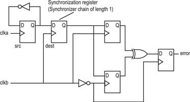
In this design, clka and clkb are two unrelated clock signals. The data input to the synchroniser toggles every clock cycle (a high fDATA). The synchroniser has length 1, because the single synchronising register feeds two destination registers. The destination registers capture the output of the synchroniser one clock cycle later and one half-clock cycle later. If the signal goes metastable before resolving at the next clock edge, the circuit detects that the sampled signals are different, and outputs an error signal. This circuitry detects a high proportion of the metastability events that occur at the half-clock cycle time.
This circuit is replicated throughout the device to reduce the effect of any local variation, and each instance is tested consecutively to eliminate any noise coupling. Altera measures each test structure for one minute and records the error count. The test is performed at different clock frequencies, and the MTBF versus tMET results are plotted on a logarithmic scale. The C2 constant corresponds to the slope of the trend line for the experimental results, and the C1 constant scales the line linearly.
Improving metastability MTBF
Due to the exponential factor in the MTBF equation, the tMET/C2 term has the largest effect on the MTBF calculation. Therefore, metastability can be improved by optimising the device’s C2 constant with architecture enhancements, or optimising the design to increase the tMET in the synchronisation registers.
FPGA architecture enhancements
The metastability time constant C2 in the MTBF equation depends on various factors related to the process technology used to manufacture the device, including the transistor speed and the supply voltage. Faster process technologies and faster transistors allow metastable signals to resolve more quickly. As FPGAs have migrated from 180 nm process geometries to 90 nm, the increase in transistor speed usually improves metastability MTBF. Therefore, metastability has not been a major concern for FPGA designers.
However, as the supply voltage reduces with reduced process geometries, the threshold voltage for the circuit does not decrease proportionally. When a register goes metastable, its voltage is approximately one half of the supply voltage. With a reduced power supply voltage, the metastable voltage level is closer to the threshold voltage in the circuit. When these voltages get closer together, the gain of the circuit is reduced and the registers take longer to transition out of metastability. As FPGAs enter the 65 nm process geometry and lower, with power supplies at 0,9 V and lower, the threshold voltage consideration is becoming more important than the increase in transistor speed.
Therefore, metastability MTBFs generally get worse unless the vendor designs the FPGA circuitry to improve metastability robustness.
Altera uses metastability analysis of the FPGA architecture to optimise the circuitry for improved metastability MTBF. Architecture improvements in Altera’s 40 nm Stratix IV FPGA architectures and new device development have improved the metastability robustness results by reducing the MTBF C2 constant.
Design optimisations
The exponential factor in the MTBF equation means that an increase in the design-dependent tMET value increases a synchroniser MTBF exponentially. For example, if the C2 constant for a given device and set of operating conditions is 50 ps, then an increase of just 200 ps in tMET makes the exponent 200/50 and increases the MTBF by factor e4, or more than 50 times, while an increase of 400 ps multiplies the MTBF by e8, or almost 3000 times.
In addition, the chain with the worst MTBF has a major affect on the design MTBF. For example, consider two different designs that have 10 synchroniser chains. One design has 10 chains with the same MTBF of 10 000 years, and the other has nine chains with MTBF of a million years but one chain with MTBF of 100 years. The failure rate for the design is the sum of the failure rates for each chain, where the failure rate is 1/MTBF. The first design has a metastability failure rate of 10 chains × 1/10000 years = 0,001, therefore the design MTBF is 1000 years. The second design has a failure rate of nine chains × 1/1000000 + 1/100 = 0,01009 and the design MTBF is about 99 years – just slightly less than the MTBF of the worst chain.
Put another way, one badly designed or implemented synchronisation chain dominates the design’s overall metastability MTBF. Because of this effect, it is important to perform metastability analysis for all asynchronous signals and clock domain transfers. The designer or tool vendor can have a very significant impact on a design MTBF by improving the tMET for the synchroniser chains with the worst MTBF.
To improve metastability MTBF, designers can increase tMET by adding extra register stages to synchronisation register chains. The timing slack on each additional register-to-register connection is added to the tMET value. Designers commonly use two registers to synchronise a signal, but Altera recommends using a standard of three registers for better metastability protection. However, adding a register adds an additional latency stage to the synchronisation logic, so designers must evaluate whether that is acceptable.
If a design uses the Altera FIFO megafunction with separate read and write clocks to cross-clock domains, designers can increase the metastability protection (and latency) for better MTBF. Altera’s Quartus II MegaWizard plug-in manager offers an option to choose increased metastability protection with three or more synchronisation stages.
Quartus II software also offers metastability analysis and optimisation features to increase the tMET on synchronisation register chains. When synchronisers are identified, the software places synchronisation registers closer together to increase the output timing slack available in the synchroniser chain, and then reports the metastability MTBF.
Conclusion
Metastability can occur when signals are transferred between circuitry in unrelated or asynchronous clock domains. The mean time between metastability failures is related to the device process technology, design specifications and timing slack in the synchronisation logic. FPGA designers can improve system reliability and increase metastability MTBF by increasing the tMET with design techniques that add timing slack in synchronisation registers.
Altera characterises the MTBF parameters for its FPGAs and improves metastability MTBF with device technology improvements. Designers using Altera FPGAs can take advantage of Quartus II software features to report metastability MTBF for their design, and optimise design placement to increase MTBF.
Acknowledgements
* Jennifer Stephenson, Applications Engineer, member of technical staff, Software Applications Engineering, Altera Corporation.
* Doris Chen, advanced software engineer, Software and Systems Engineering, Altera Corporation.
* Ryan Fung, senior member of technical staff, Software and Systems Engineering, Altera Corporation.
* Jeffrey Chromczak, senior software engineer, Software and Systems Engineering, Altera Corporation.
For more information contact EBV Electrolink, +27 (0)21 402 1940, [email protected], www.ebv.com
| Tel: | +27 11 236 1900 |
| Email: | [email protected] |
| www: | www.ebv.com |
| Articles: | More information and articles about EBV Electrolink |


© Technews Publishing (Pty) Ltd | All Rights Reserved
 printer friendly version