


Similarly to Moore’s Law [1] of semiconductors, stipulating that approximately every 18 months the number of transistors per chip is doubled, one has experienced a doubling each year of the required bandwidth for backplanes and systems in the last 10 years [2]. This 'bandwidth hunger' is driven mainly by telecom/datacom applications and intensive computing graphics in the PC sector.
For a traffic light control or industrial application even today, an ISA bus would still be sufficient, yet the old ISA chipsets are no longer available. And therein lies the problem. The present chipsets for parallel buses, too, will no longer be obtainable in the near future. Where high-speed backplanes were a novelty a few years back, tomorrow they will be present in each traffic light controller. Everyone that works with backplanes will need to grow accustomed to this trend.
From unusual to commonplace
Until recently, industrial applications were configured with the low pulse frequency of parallel buses, such as VMEbus, CompactPCI or solely on a PCI basis. In telecommunications networks serial transfer protocols with differential transfer paths have been dominant for some time, but the data volume was considerably lower than today.
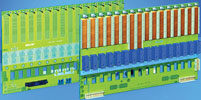
The problem with the design of high-speed backplanes (Figure 1) is heightened by the change in technology which is taking place at present. All upgrades of parallel buses were more or less downward compatible. The recent VMEbus boards not only supported 2eSST protocols, but also the old BLT protocols combining different speeds in one system. Though, with (Compact)PCI, the slowest board governs the speed of the system, new and old boards, too, can co-exist and operate in one system. Until recently there was no need during the design of backplanes or a system to compete with higher transfer volumes.
With the changeover from parallel to serial transfer topologies, such as PCI Express (PCIe), Ethernet, SerialATA (SATA), Infiniband, serial Rapid I/O and others, hardware compatibility no longer exists. Therefore a change to high-speed backplanes is enforced and each system architect is advised to base new designs on serial transfer topologies. The old chipsets will barely be available in the near future.
The positive aspect of this scenario is the software compatibility. The application does not care whether it communicates with a parallel bus or a serial packet orientated interface. The user software runs the same as it always did, only the backplane designers face new challenges. Therefore, from the side of the user, there is no reason not to change to the new serial protocols and to protect the backplane designer from the torture of high-speed designs.
New design guidelines are necessary
Multigigabit backplanes are still subject to the same laws of physics as their predecessors, but the conventional design guidelines fail. They are always based on certain simplifications, which after a jump over two or three decades, from 'MHz' to 'GHz', are no longer tolerable. Losses in the dielectric and through the skin effect are beginning to play a big role. But even more critical is the configuration of the vias, the connection of the backplane to the outer world. Through-connections, into which mostly connectors are pressed-in, create problems seen from several viewpoints, which could still be ignored with old 'MHz' buses:
* Through the stub effect, serial resonances are generated, which drain the energy of the signal.
* The large capacitance causes a strong impedance discontinuity, which generates reflections and worsens the signal-to-noise ratio.
* Through the high capacitance, the via acts like a low-pass filter and filters the high frequency signals which are required for the transmission of serial protocols.
Serial resonances are generated
So-called serial resonances, also known as stub effect or Lambda quarter resonance, virtually 'suck' energy from the signal and can by far exceed the dielectric and skin effect losses with their influence on the signal integrity. These resonances are created when the signal splits at a 'junction'.
Part of the signal energy, led from the connector over the insertion zone or the SMD contact to the via, is transferred from the via as planned to the conductive path. Another part of the energy, however, runs along the via, past the conductive path, up to the end of the via at the other side of the backplane. There the energy is reflected and only then transferred to the conductive path.
Relative to the length of the via, these signal components - the one directly transferred to the conductive path and the one taking the detour over the via - have a time lapse or phase difference. If the phase difference reaches 180°, the spectral port of the signal is effectively erased and nothing reaches the receiver. This phase displacement is dependent on the operating frequency, so that a 180° phase shift corresponds to half a period according to the formula T = 1/f. Therefore, the speed of the signal in the via determines the frequency at which the signal is extinguished.
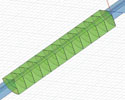
Apart from the geometric difference in length, the resonance frequency also depends on the speed with which the signal spreads. This is considerably lower in the via than in the homogenous dielectric and is determined by the parasitic capacitance. The geometric conditions can be calculated easily. The contact point of the insertion zone of the connector is known, as is the total thickness of the backplane and the vertical position of the conductive path. Measurements on the finished product provide help for a re-design. 2D or even 2½D field calculations are not sufficient in order to describe complex three-dimensional configurations like vias. Only calculations from the first design combined with 3D field calculation software solve the problem quickly and cost effectively [3] (Figure 2).
Backdrilling
A common technique for changing the resonance frequency to higher values is so-called 'backdrilling' or 'counter boring'. When this is carried out, the resonance frequency has less influence on the chosen data transfer rate. The via is drilled out at the back of the board and appears electrically shorter. The manufacturing costs of the boards are only influenced very moderately by this. The number of drillings plays a role, as well as the number of the different drill depths or backdrill levels, since the drilling machine has to be re-adjusted for each drilling type. Even if the backdrilling sounds simple, the technology is not yet in widespread use and is only carried out reliably by a few manufacturers. During the design phase, an agreement with the board manufacturers and the observation of the design guidelines [4] are highly recommended.
Reduction of the number of drill depths
It is not always necessary to define a backdrill level for each layer of the board. It is up to the designer to get a good overview during the simulation in order to compromise when choosing the different drill depths. Depending on the thickness of the board and the highest data volume, one or two drill depths could be sufficient and thereby save costs. For data volumes above 6 Gbps, however, a somewhat finer adjustment of the drill depths would be required.
A further measure to control costs is the controlled distribution of the connections onto certain layers of the backplane. With this, some of the backdrillings can be avoided altogether or the number of drilling depths can be reduced. Short conductive paths have clearly lower dielectric and skin effect losses. If the loss budget is not used up, the losses through the stub resonance can be higher and one backdrill level can be dropped.
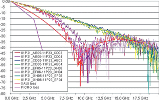
The physical background to this is that the resonance point on the frequency scale is not very clearly pronounced. Even before or after the actual resonance, the suppression is larger in comparison to a conductive path in the homogenous dielectric. One less backdrill level - or at another depth than the maximum - changes the resonance point more or less to lower frequencies. Therefore, the suppression increases at lower frequencies, without resulting in signal cancellation. A simulation of loss carrying conductive paths, fed with models from the three-dimensional field calculation of the via configuration, not only helps for re-designs, but also to save direct costs for individual boards. Figure 3 shows the input suppression of conductive paths with and without a resonance point.
Vias and impedance jumps
When the signal is directed to the 'base' of the backplane, the serial resonance does not appear any longer, but the large parasitical capacitance of the vias is still active and lowers the impedance in the via dramatically. This results in impedance jumps along the length of the entire path from the sender to the receiver. Unfortunately with this discontinuity, a considerable part of the signal energy is reflected.
Signal parts already reflected on the first via, do not enter the backplane and can therefore not reach the receiver. This effect cannot be counteracted with more expensive board materials with lower dielectric losses. Energy which has not been fed into the system cannot be transferred, not even with a superconductor. But materials which generate fewer losses will improve a bad design for the actual transfer volume and for the next generation.
A further part of the signal energy is reflected along the next via and runs back and forth in the backplane. These reflections interfere with the desired signal, thereby worsening the signal-to-noise ratio and increasing the jitter - the measure of time needed for the signal transfer between two logical levels - considerably. Both effects make the recognition of the signal in the receiver more difficult and, together with the other effects described, can finally result in the loss of the signal.
Vias are low-pass filters
Due to their large parasitic capacitance, the vias act like low-pass filters. They filter the high frequency signal parts, which in contrast to the slow 'MHz' buses are now required for the signal transfer. A common method to alleviate the problem is to leave out the pads that are not connected to a conductive path (non-functional pads), a function supported by many CAD systems when manufacturing data are issued. Otherwise the designer should forego 'universal' pads and define a separate one for each signal position.
Configuration of large antipads
Another measure is obvious: to design the clearances in the reference layers (antipads) as large as possible. But this, too, is a compromise. Generally, conductive paths are positioned between the connector drillings and they should be covered by a reference layer on both sides. This sets a natural limit to the enlargement of the antipads. In a simulator the most diverse scenarios can be created before the best compromise is applied in the final design. The effect of clearances in the reference layers (antipads) can partly be compensated for by the stray capacitance from the via to the conductive path. So the via diameter, the horizontal distance of the conductive path from the via and the diameter of the antipads are all linked.
Lower impedance values for differential lines
The first step to improve the situation, as previously described, is the reduction of parasitic capacitances, ie, a general optimisation of the via for the individual configuration of layers. Simulations show, however, that it is nearly impossible to design vias with an impedance of 50 Ω for the current connectors. This leads to consideration of the common impedance value for single lines of 50 Ω (100 Ω for differential pairs) and to question them.
A value of 80 to 90 Ω for differential lines, or 40 to 45 Ω for single ended lines, in the entire path from sender to receiver, could definitely be a solution for the transmission of higher data volumes. These impedance values, approximately 40 or 80 Ω, could be achieved for vias in backplanes with a careful design at justifiable costs. If then the entire path is configured at this impedance, the losses through reflection are reduced considerably, which with conventional designs can clearly be more than 50%. If other losses and interference effects are minimised, too, transfer volumes of 10 Gbps and more can be realised in copper.
Equal signal run time
A further problem during the design of high-speed backplanes is the different signal run times (skew), in both lines of a differential pair and also between differential pairs. In order to be able to detect a signal which already arrived significantly weaker at the receiver through the effects mentioned, only a very minute time lapse, as a rule in the region of a few picoseconds, is tolerable.
The easiest way to counteract this, but also the precondition for a minimum time lapse, is to use lines of equal lengths; this is supported by all current CAD systems, so it is trivial and really only a question of diligence. Even if a backplane has been designed following these guidelines, as a rule a time lapse can still be found in the finished product, which can even exceed the protocol and data dependent limits. Why?
The board material is largely homogenous in its volume, but not in the micro area around the conductive path. The material is strengthened with fibreglass of different structure and the conductive paths do not have a defined position and orientation to the fibre strands. Furthermore, as the dielectric constants of glass and resins are very different, the orientation of the individual conductive path to the fibre strand plays a big part.
Also, the electric field around the conductive path is not homogenous, it is stronger nearby than at a larger distance (~1/R²). Therefore, the fibreglass strands near the conductive path have a bigger influence than those strands which are further away. To solve this problem is relatively difficult. Wider conductive paths and finer fibreglass strands may be the only possibility to reduce the problem.
Observation of copper distributions
A further influence is non-homogenous copper distributions. If for instance one differential line pair is led symmetrically through a connector via field, both lines of the pairs are exposed to the same stray capacitance field of via columns and pads (Figure 4). But if two line pairs are led through the same via field, the capacitance of the outer lines is clearly more stretched than the inner lines (Figure 5).


The same applies to a differential line which is led outside the via field, but near enough to the last via row. If there are only a few vias where the line is led, the influence is minimal. If, however, the line passes many vias, like for instance with a full mesh backplane, the effect accumulates to impose a considerable influence on the time lapse between the two individual lines. The designer can only take care that both lines in a differential pair always 'see' the same amount of copper.
Summary
Through the probably very fast change from parallel interfaces to packet orientated serial transport mechanisms, each backplane design will become a high-speed design, independent of the current 'speed' requirement of the application. The design of high-speed backplanes is not trivial nowadays. Many old and well established design guidelines are no longer valid.
There is added difficulty in that the effects mentioned cannot easily be predicted by simple means, ie, without 3D field assessment and simulation of loss carrying lines. In a few years designers will probably no longer think about these questions, because their solutions will have become current technology like the design of VME or CompactPCI backplanes today.
Where and when 'high-speed' will end is difficult to envisage... At IEEE, a working group was recently formed that prepares the standardisation of 100 Gigabit Ethernet.
References:
[1] IEEE solid-state circuits society newsletter; 'The Technical Impact of Moore's Law'; September 2006.
[2] IEEE 802 March 2007 Plenary Week; IEEE 802.3 Higher Speed Study Group Meeting, March 12 15, 2007, Orlando, FL.
[3] G. Selli, et al.; Developing a 'Physical' Model for Vias, DesignCon 2007.
[4] Jürg Haas; Back Drilling Design Guideline; PPC Eletronic AG.
| Tel: | +27 11 608 3001 |
| Email: | [email protected] |
| www: | www.actum.co.za |
| Articles: | More information and articles about Actum |


© Technews Publishing (Pty) Ltd | All Rights Reserved
 printer friendly version