Achieving compact PCB footprints and high DC-DC converter efficiency requires careful attention to high-voltage device integration and process technology selection.
Since the IEEE Std 802.3af, or Power-over-Ethernet (PoE) standard was ratified in June 2003, millions of PoE-enabled VoIP phones, WAPs (wireless access points) and security cameras have shipped worldwide. PoE is being built into a wide array of applications, such as point-of-sale terminals, networked sensors and building automation, because it conveniently and simultaneously delivers data and power.
Projected shipments of PoE-enabled products for power sourcing equipment (PSEs) and powered devices (PDs) will exceed 100 million ports in 2008. While a substantial number, these 100 million ports represent less than one third of all wired Ethernet port shipments in 2008. Reducing the design effort and incremental cost of adding PoE to new and existing Ethernet products will encourage even higher levels of PoE adoption.
One approach to facilitate simpler, more compact and less costly PoE PD solutions is to integrate the high-voltage, typically discrete, silicon components. Multiple diode bridges, a transient voltage suppressor (TVS), and a power MOSFET for the PWM switching regulator are examples of components which can be integrated, but are typically not due to the complex nature of high voltage integrations. This article provides an overview of key system-level requirements one must consider when integrating these devices into a PoE PD interface and power management controller - and the resultant benefits.
Today's solutions
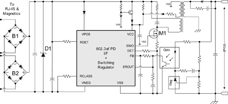
Powered device interfaces for PoE-enabled products have evolved from the early, fully-discrete implementations to the current generation of single-chip solutions that integrates the detection, classification and hot swap interface functions (required by the IEEE 802.3af standard), and a companion pulse width modulator (PWM) for DC-DC conversion. A typical solution is shown in Figure 1, including the external components required for a common isolated power supply.

The flyback regulator topology is widely used because it provides electrical isolation between the input PSE and output PD power supplies and supports the 2 W to 10 W power profiles of today's two primary PoE applications: VoIP phones and WAPs. Many PD applications require more than one regulated supply; so, multiwinding transformers, LDOs or buck post regulators often generate the supply voltages for the PD's radio, processor and other subsystems.
Typical solutions require approximately 35 to 50 external components. Although many are relatively inexpensive resistors and capacitors, about 8 to 10 high-voltage and/or high current active devices increase PCB footprint size and bill-of-materials (BOM) cost. These components are:
* Line side diode bridges - either six or eight discrete diodes or two integrated full bridge rectifiers (B1 and B2 in Figure 1).
* Transient voltage suppressor (TVS) - typically a single SMAJ58A or similar zener diode clamp (D1 in Figure 1).
* Switching regulator power MOSFET(s) - one or two devices depending on the PWM architecture (M1 in Figure 1).
Integrating high-voltage devices into the powered device interface simplifies the overall PD design and minimises the external BOM. The subsequent benefits are seen by examining how each of these three devices functions in a PD, the relevant IEEE Std 802.3af specifications that dictate performance, and what kind of process technology might permit integration of these high-voltage functions.
The critical line side diode bridges and TVS clamp
Generally external and discrete, the diode bridges and the TVS are important components that provide electrical overstress protection in the harsh PoE operating environment. While functionally straightforward, the diode bridges on the line side of the PD interface must provide the following critical functions:
1) Efficiently connect the PSE supply to the PD interface, regardless of the supply polarity on the cable.
2) Safely handle the full operating voltage and current ranges, as defined by IEEE Std 802.3af.
3) In tandem with the TVS diode, withstand potentially damaging transient surge events, as defined by IEC-60060, or those generated by cable discharge events (CDE).
From an operating voltage range perspective, the diode bridge must simply connect the 44 V to 57 V d.c. supply from the power sourcing equipment (PSE) to the PD interface. For the centre tap nodes (CT1/CT2), the 802.3af specification mandates that the PD must accept power of either polarity. This requirement necessitates the use of one complete diode bridge, or four diodes, for the CT1 and CT2 pins, which are normally connected to the data pairs in 10/100BASE-T applications.
For the spare pairs (SP1/SP2), the IEEE specification explicitly defines the polarity of the PSE supply voltage - so only a half bridge is technically required. However, since transient events from ESD, cable discharge, or induced lightning surges occur in either polarity, prudence dictates choosing a full bridge for the spare pair inputs. If a surge hits the spare pairs without a full bridge, the interface could end up seeing voltages above 1 kV, which could break down and destroy the diodes.
Using a full diode bridge also allows any input (CT1/CT2/SP1/SP2) to be hooked up to any output from the Ethernet transformer or RJ-45 to mitigate any potential wiring mistakes in the cable. The IEEE specification defines an input operating current of 350 mA and a maximum in-rush current limit of 400 mA. Assuming sufficient design margin, the bridge diodes must handle up to 500 mA of DC current over the full operating temperature of the powered device.
As noted earlier, the diode bridge and TVS must be able to withstand transient surges specified in IEC-60060. A surge event is defined as a 1000 V impulse of either polarity applied across CT1-CT2 or SP1-SP2. The shape of the impulse is a 300 ns full rise time and a 50 μs half fall time, with 201 Ω source impedance. As a result, during surge events, the TVS diode may experience up to 5 A of transient current. This is essentially the peak pulse current specification, or IPP, for a discrete TVS device.
To meet the bridge and TVS functional requirements, integration of these critical components requires a process technology that provides both high operating voltages and electrical isolation between the PSE supply and the rest of the PD interface. Of course, cost compared to a discrete implementation must also be considered.
A look at the switching regulator power MOSFET
Many switching regulator controllers do not integrate the power MOSFET. The resulting flexibility of input voltage range and output power range comes at the cost of switching efficiency, PCB footprint, and cost optimisation. Since the PoE PD input voltage range (36 V to 57 V) and output power (12,95 W max) fall within a fairly narrow profile, designers may feasibly integrate an application appropriate switching power FET.

RSP is a figure of merit commonly used for describing the on-state resistance capability of a technology. With units of Ωmm², RSP is the product of a MOSFET's on-resistance (RDSon) and its total layout (not just the gate) area. The lower a MOSFET's RSP, the smaller the device necessary for achieving a target RDSon. External high-voltage MOSFETs are generally constructed using more mature technologies with relatively high RSP, meaning the devices can be quite large to achieve low on-resistance. Furthermore, full-channel inversion (and thus lowest on-resistance) occurs at relatively high gate voltages.
These two factors - high RSP and high gate voltages - create the primary loss of switching efficiency seen when using an external power MOSFET. Not only do external FETs introduce PCB parasitics, but the large device area creates appreciable gate capacitance which the controller must charge and discharge when turning the FET on and off. Since switching power is proportional to CGATEVGATE², external MOSFETs can consume considerable excess power if not properly sized for the PoE application.
With prior knowledge of the voltage specification and output power range, an optimally-sized switching power MOSFET in an appropriate technology dramatically reduces these issues. FET on-resistance and gate-area tradeoffs converge on the best possible device architecture. Combined with smaller voltages on the gate, significant power savings may be realised. Integrating the FET into a small package with its control circuitry enables a PD solution with a smaller form factor than a discrete solution.
Summary of process requirements for high-voltage integration
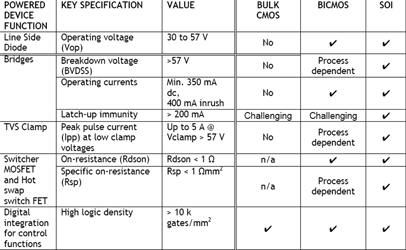
The general specifications for the diode bridge, TVS clamp, switcher FET, and digital control circuitry are summarised in the first three columns of Table 1. The last three columns compare these powered-device specifications with the abilities of three commercially available process technologies to integrate these requirements.

Based on these specifications, it is evident that mainstream, bulk CMOS and BiCMOS technologies fall short of the optimal mix of high-voltage, power and efficiency for the PD application.
However, silicon-on-insulator (SOI) technology offers high-performance junction devices, such as diodes and BJTs, while providing the area and efficiency of power MOSFETs. Furthermore, SOI's robustness in the presence of significant high-power transients and inherent internal noise isolation ease the integration of high-quality power devices and precise digital and analog control. Deep trench isolation and buried oxides eliminate the dangerous parasitics and bulky junction-isolation barriers seen in the other technologies.
The ideal solution for PoE involves high-voltage integration
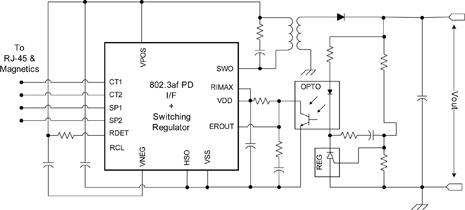
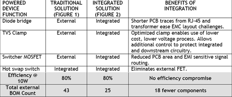
High-voltage integration must have real-world benefits to be of value to the PoE PD system designer. Lower total BOM component count is a good indicator of cost and conversion efficiency, which are two tangible real-world benefits for designers. Contrasting with the traditional solution in Figure 1, the circuit in Figure 2 illustrates a solution based on the SOI process.

An additional benefit of an integrated surge suppressor is that a lower clamping voltage can be utilised, avoiding the need for a process with a higher breakdown voltage. For example, at IPP = 5 A, a standard SMAJ58A will clamp to around 94 V - necessitating a 100 V capable process for the PD interface IC. With access to all electrical nodes, an integrated TVS solution can coordinate the shunting of all high-current transients through the TVS diode. For example, when tripped, the internal TVS actively disables the hot-swap interface and switching regulator, preventing downstream circuits from encountering potentially damaging high-energy transients.
Through novel application of high-voltage circuit design techniques and utilisation of an SOI process technology, a more highly-integrated PD power supply solution eliminates 18 or more external components while delivering high efficiency as compared to a discrete solution.
| Tel: | +27 11 608 0144 |
| Email: | [email protected] |
| www: | www.nuvisionelec.com |
| Articles: | More information and articles about NuVision Electronics |
© Technews Publishing (Pty) Ltd | All Rights Reserved