


Attaining high performance and low power consumption in portable consumer applications has long challenged designers.
These battery-powered systems typically employ an embedded digital signal processor (DSP) to achieve maximum processing power when handling multimedia applications and minimum power consumption when in sleep mode. Battery life is of prime importance in handheld battery-powered products, making their success directly related to the efficiency of the power system.
A key component of such systems, a step-down DC-DC switching regulator, efficiently derives a low supply voltage, say 1 V, from a higher voltage supply, for example 4,5 V. As a regulator, it must maintain a constant voltage, rapidly responding to variations in the upstream supply or the load current. This article discusses an architecture that provides good regulation, high efficiency and fast response.
Anatomy of a switching regulator
Figure 1 shows a typical application circuit using the Analog Devices ADP21021 low-duty-cycle, 3 MHz, synchronous step-down converter. It is available with a number of fixed-output and resistor-programmable voltage options. Here it is connected in a fixed-voltage configuration, producing a regulated 0,8 V output from a 5,5 V input voltage and driving a 300 mA load.
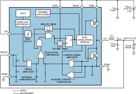
Here is a brief explanation of the circuit's operation: a fraction of the DC output voltage is compared with an internal reference in the error amplifier, whose output is compared with the output of a current-sense amplifier to drive a one-shot that is on for a period of time that depends on the ratio VOUT/VIN. The one-shot turns on the upper gating transistor and the current in inductor L1 ramps up. When the one-shot times out, the transistor is turned off, and the current ramps down. After an interval determined by the minimum-off-timer and the minimum ('valley') current, the one-shot is pulsed again. The on-chip one-shot timer employs input voltage feed-forward to maintain a constant frequency in the steady state.
This oscillation continues indefinitely - at approximately 3 MHz, but deviating as necessary to respond to transient line and load changes - maintaining the output voltage at the programmed value and the average inductor current at the value required by the output load.
The approach described above is relatively new. For many years, the principal approach to DC-DC conversion has been a constant-frequency peak-current approach, also known as trailing-edge modulation when implemented in step-down DC-DC converters.
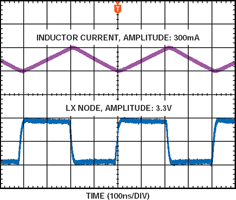
Figure 2 shows typical waveforms under various conditions. Figure 2a shows the low duty cycle that accompanies the large voltage reduction from VIN = 5,5 V to VOUT = 0,8 V at ILOAD = 600 mA. As can be seen in the plot, the minimum on-time achieved is 45 ns with a switching frequency of 3 MHz.
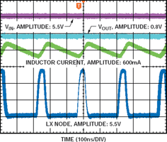
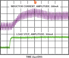
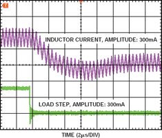
Figure 2b shows the load current and inductor current in response to a 300 mA step increase in load current. Figure 2c shows the load current and inductor current in response to a 300 mA step decrease in load current. Figure 2d shows that there are no sub-harmonic oscillations when the part operates at a 50% duty cycle, which is a concern for parts using peak-current-mode control. This freedom from sub-harmonic oscillations is also the case for duty-cycle values somewhat greater or less than 50%.
Dynamic voltage adjustment in a DSP application
In portable applications employing digital signal processors (DSPs), switching converters typically provide the DSP's core voltage and I/O rails. Both supplies require high-efficiency DC-DC converters that are designed for battery applications. The regulator that supplies the core voltage must be able to change the voltage dynamically based on the processor's clock speed or as directed by the software. Small total solution size is also important.
Described here are improvements in system power efficiency that can be attained in battery-powered applications by replacing a Blackfin processor's internal regulator with an external high-efficiency regulator. Also described is the control software for the external regulator.
Dynamic power management
A processor's power dissipation is proportional to the square of the operating voltage (VCORE) and linearly proportional to the operating frequency (FSW). Thus, decreasing the frequency will lower the dynamic power dissipation linearly, while reducing the core voltage will lower it exponentially.
Changing the clock frequency - but not the supply voltage - in a power-sensitive application is useful when the DSP is simply monitoring activity or waiting for an external trigger. In high-performance battery-powered applications, however, merely changing the frequency may not save enough power. Blackfin processors, and other DSPs with advanced power-management features, allow the core voltage to be changed in tandem with frequency changes, thus seeking optimal loading of the battery for each situation.
Dynamic voltage regulation in ADSP-BF53x3 series Blackfin processors is typically implemented with an internal voltage controller and an external MOSFET. The advantage of this approach is that a single voltage (VDDEXT) can be applied to the DSP subsystem, while the DSP derives the necessary core voltage (VDDINT) from the MOSFET. Internal registers allow the regulated core voltage to be software controlled in order that the MIPS, and ultimately the consumed energy, can be coordinated to achieve optimal battery life.
To fully implement this internal Blackfin regulator scheme requires an external MOSFET, a Schottky diode, a large inductor and multiple output capacitors - a relatively expensive solution with poor efficiency that uses a relatively large PCB area. The use of the large inductors and capacitors required by the integrated regulator brings the system designer into conflict with consumer desires for portable devices to be as small as possible. Along with the relatively low efficiency of the integrated regulator controller - typically 50% to 75% - this approach is less than optimally suited for high-performance, handheld, battery powered applications.
External regulation
The native efficiency of the Blackfin integrated approach can be improved to 90% or more by designing in a modern DC-DC switching converter. The size of the external components can also be reduced when an external regulator is used.
A variety of dynamic voltage-scaling (DVS) control schemes are available, ranging from switched resistors - which in some cases can be implemented by using a DAC - to pulse-width modulation (PWM), which can achieve as fine a granularity as the internal method. Whatever scheme is used must provide the ability to change the regulation level via software control. While this regulation control method is inherent with the internal regulator approach, it must be added in external approaches.
This article describes two ways to adjust the DSP's core voltage by using an ADP2102 synchronous DC-DC converter to dynamically adjust the core voltage to values from 1,2 V to 1,0 V when the processor is running at a reduced clock speed.
Figure 3 illustrates a circuit that implements DVS. A 3,3 V system power supply powers the ADP2102 buck converter, whose output voltage is set to 1,2 V using the external resistive dividers R1 and R2. A GPIO pin from the DSP is used to select a requested core voltage. Varying the feedback resistor adjusts the core voltage from 1,2 V to 1,0 V. An N-channel MOSFET modifies the voltage divider by inserting resistor R3 in parallel with R2.
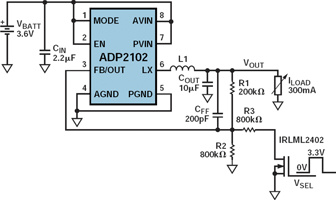
The 0,25 Ω RDSon of the IRLML2402 is small compared to R3. The 3,3 V GPIO voltage is used to drive the MOSFET gate. Feed-forward capacitor CFF is needed for better transient performance and improved load regulation.
The general application requirements for two-level switching are:
1. DSP core voltage (VOUT1) = 1,2 V.
2. DSP core voltage (VOUT2) = 1,0 V.
3. Input voltage = 3,3 V.
4. Output current = 300 mA.
High-value resistors are used to minimise power losses through the resistive divider. The feed-forward capacitor reduces the effect of the gate-to-drain capacitance during switching. The overshoot and undershoot caused during this transition can be minimised by using smaller feedback resistors and a larger feed-forward capacitor, but only at the expense of additional power dissipation.
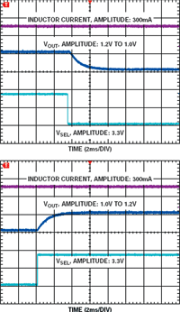
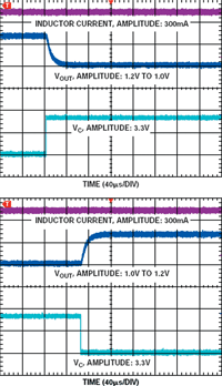
Figure 4 shows the output current, IOUT, output voltage, VOUT, and control voltage, VSEL. A low level on VSEL scales the output voltage to 1,0 V, and a high level on VSEL scales it to 1,2 V.
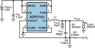
A simpler way to generate two different voltages for DVS uses a control voltage, VC, to inject current into the feedback network through an additional resistor. Adjusting the duty cycle of the control voltage varies its average DC level. A single control voltage and resistor can thus be used to adjust the output voltage. The following equations are used to calculate the values of resistors R2, R3, and the control voltage amplitude levels, VC_LOW and VC_HIGH.

With VOUT1 = 1,2 V, VOUT2 = 1,0 V, VFB = 0,8 V, VC_LOW = 3,3 V, VC_HIGH = 0 V, and R1= 49,9 kΩ, R2 and R3 can be calculated as follows:

This approach produces much smoother transitions. Any control voltage that can drive resistive loads can be used for this scheme, as opposed to the MOSFET switching approach, which can only be used with control signal sources that can drive capacitive loads.
This approach can be scaled to any output voltage combinations and output load currents. Thus, DSP power dissipation can be reduced by scaling the core voltage as needed. Figure 5 shows the implementation of the above scheme. Figure 6 shows the transition between the two output voltages using this current injection method.


© Technews Publishing (Pty) Ltd | All Rights Reserved
 printer friendly version