


With rising consumer demand for smaller high-function portable electronic devices, it becomes ever more critical to creatively arrange circuits and components to support operation, while satisfying cost and manufacturing assembly yield targets.
While 0201 size resistor and capacitor components continue to grow in popularity to meet stricter form factor design constraints, the emergence of the 01005 passive is yet an even smaller size option now being offered. The assembly process concerns between 0201 and 01005 are quite similar, however common expectation is that the smaller 01005 should behave more sensitively to process and design variables. There have already been several articles published on 01005 assembly and the common conclusion between these is to recommend fine powder solder paste (Type 4 or 5) used in conjunction with a thin stencil
(3-mils)1,2,3. It is the motivation of this work to challenge the previous two recommendations and prove or disprove that the 01005 assembly process can be performed successfully with Type 3 powder size standard solder paste material using a 4-mil thickness stencil. This data should be useful to the typical SMT manufacturer who is already using Type 3 solder paste and may also be facing stencil thickness reduction to 4-mil thickness to accommodate small CSP and 0201s.
Test results
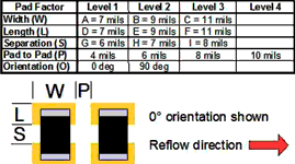
What follows are some of the more significant results of the extensive range of tests conducted as part of this work. The 01005 components used for assembly were resistor types only. The termination metal on these passives was 100Sn. Table 1 shows the pad designs used during these tests.
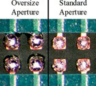
Inspection of the reflowed boards showed no bridging, very low occurrence of solder balls and no open solder joints. This introduces evidence that a wider than expected pad and stencil design process window may exist to achieve high yield 01005 resistor assembly using both SAC305 and eutectic Sn/Pb solder. Several pad designs printed with the 'oversize' apertures that were assembled showed instances of floating components. An example of this is shown in Figure 1.
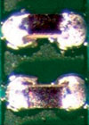
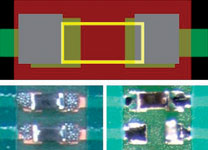
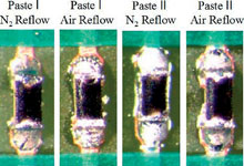
Figure 2 shows a comparison between leaded and non-leaded solder paste assembly on pad design BEG using the largest paste grab 'standard' aperture design at 4-mil pad spacing. Note the significant difference in wetting between the two alloys. Even with a high concentration of nitrogen present in reflow, the lead free solder paste tends to form bulging solder joints at the terminations due to reduced wetting.
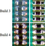
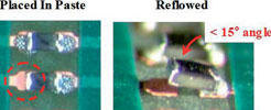
Figure 3 shows a pad design BEI with simulated 1,0 mil diagonal offset print and accurate 01005 placement. The west positioned paste deposit barely contacts the left termination, while the east positioned paste deposit still overlaps the right termination. The grab imbalance caused by the print misregistration at this pad separation and lowest designed stencil grab level creates a condition that favours paste climbing the right termination during reflow and pulling the component to the tombstoned state as shown. Pb-free paste has shown more resistance to tombstoning, likely explained be a weaker wetting force being exerted on the terminations, allowing greater tolerance for paste misregistration and grab imbalance.
When the previous test was repeated with air instead of nitrogen as the atmosphere profile, significantly defective results were produced - see Figure 4. Nearly all deposits showed incomplete solder coalescence. Larger deposits, particularly on the largest width pads, show better results. Assembly yield conclusions for this test were unfeasible due to challenges with reflow.
Some differences between the lead-free solder pastes from different vendors were noticed, with different behaviour in nitrogen and air reflow performance, as shown in Figure 5. No occurrences of shorting or solder balling defects were witnessed. As aperture sizes were reduced however, apertures can become totally clogged at low area ratios so that only one component termination is placed into solder. This condition was observed to produce no instances of tombstones, but did result in a few occurrences of low angle draw-bridging, as shown in Figure 6.
With the unexpected absence of open solder joints from all previous tests, the purpose of further tests was to study the tombstone trends between two Pb-free solder pastes on the effect of printing solder on only one of the two termination attachment pads for both 0201 and 01005 resistors. Surprisingly, the frequency of tombstones occurring on 0201 resistors is much greater than 01005s when the reflow atmosphere is nitrogen. This observation was consistent with both vendors' pastes using their respective unique thermal profiles. Figure 7 shows a typical view of 0201s and 01005s from an assembled board that was reflowed in nitrogen.
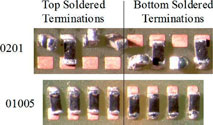
The occurrence of tombstones across both passive types was nearly the same level when the reflow atmosphere was switched to air. Although both component types showed greater resistance to tombstoning when reflowed in air, the effect of inerting the reflow atmosphere is significantly more influential on causing 0201s to tombstone. There was no correlation found to show the influence of aperture size on tombstone trends for either 0201 or 01005 components.
Recommendations
The following designs are suggested for 01005 resistor assembly compatibility with stencil thickness of 4 mils and Type 3 solder paste. The ranking strategy for pad designs is shown in Table 2.
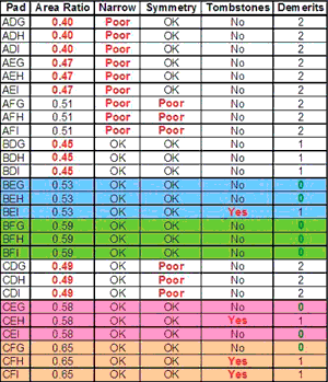
There are four categories used to evaluate the designs. Only 'standard' aperture sizes are considered, with designs having print area ratio below 0,5 scored with a demerit, indicated by red font. The second category labelled 'narrow' compares the pad width dimension to the 01005 resistor width. Due to all the pad width 'A' designs being narrower than the component width, these are all designated 'poor' as this scenario is not generally advised. The third category is 'symmetry' which assigns demerits to aperture designs that are most rectangular. The logic here is that more non-symmetrical apertures will have unequal print transfer results comparing 0ø and 90ø orientations. The final category of tombstones represents locations where this occurs on Build 3 in Figure 2. A count of all the demerits (red labels) is shown in the final column. The summation of demerits is used to determine the qualified pad and stencil designs.
The top three pad and stencil designs are BF, CE, and BE. Ranking in this order follows area ratio from high to low, so BF should produce better print results than the other two designs. Of the three pad separations, level 'G' did not show any tombstone defects and is considered the recommended design. At pad separation 'G' the influence of aperture grab level was not found significant on causing defects. The highest aperture design grab level 'H', where apertures are centred on the pads, is suggested as this should help to relax print and placement accuracy requirements.
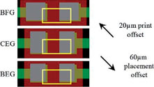
Pad designs BFG, CEG, and BEG and 'standard' size high grab stencil aperture designs are all capable of comfortably tolerating ± 20 μm print and ± 60 μm placement misregistrations while still maintaining component contact into printed solder deposits. The worst-case scenario is shown simulated in Figure 8. Larger pad separation and/or lower aperture grab designs will further challenge the ability of this offset scenario to recover in reflow.
With concern on achieving sustained consistent paste transfer results for low area ratio apertures, there are some additional changes that can increase printing success. The upgrade to electroformed stencils should increase print process stability, offering lower surface roughness aperture walls to encourage highest paste release efficiency performance4. Another enhancement is replacing the squeegees with modern low friction metal blade options that are commonly available4. Such materials improve solder paste roll circulation during the print and also reduce the tendency for paste to pull off the stencil when the squeegee is retracted after completing the print. Enclosed print head technology can also be used in place of squeegees to provide a boost to transfer efficiency performance5.
The performance of 'oversize' aperture designs was broadly successful in achieving repeatable high transfer efficiency solder deposits. However, the prevailing flaw with this stencil design strategy was the delivery of excess solder to pads, causing bulging solder joints and the occasional floating component. The only pad design recommended for use with the oversized aperture is pad design BD. Again the lowest pad separation 'G' and highest grab aperture design are advised.
Conclusion
A successful 01005 resistor assembly process has been demonstrated using a 4-mil thick stencil with both Type 3 leaded and lead-free alloy solder pastes across a variety of Cu/OSP pad sizes. A side-to-side pad spacing as low as 4-mil shows promising assembly yield results. The pad design BFG with 9,0 mil wide x 10,0 mil long apertures centred on pad is recommended. The 01005 resistors assembled with lead-free solder are found to be significantly less sensitive to tombstoning when reflowed in nitrogen compared to 0201 resistors assembled in the same manner. Similar defect ratios are found between the two component types if reflow is conducted in air. A lead-free air reflow 01005 assembly process is considered the most desirable industry practice and proof of achieving this has been realised. However this work also reveals observations of incomplete solder coalescence, suggesting that air reflow compatibility challenges may exist with small lead-free solder deposits.
Acknowledgements
Thanks to Ashok Viswanathan from Binghamton University for assistance with the component assembly process and many constructive discussions that helped shape this work. Also compliments to the staff of the Unovis Advanced Process Laboratory for supporting the assembly and inspection equipment requirements to complete this project.
References
1. Mattsson, F., Geiger, D., Shangguan, D., and Castello, T., 'Design and Assembly of 01005 Passives Using Pb-Free Solder', Circuits Assembly, 2005, 16, 5, pp 22-27.
2. Grundy, P. and Magnell, M., 'Process Optimization of an 01005', Surface Mount Technology, 2006, 20, 5, pp 26-28.
3. Borkes, T. and Groves, L., 'Process Characterization of the 01005 (English) Component Package', Proceedings from the SMTA International Conference, September 2006, Chicago, IL.
4. Coleman, W.E. and Burgess, M.R., 'Choosing a Stencil', Surface Mount Technology, 2006, 20, 7, pp 14-17.
5. Mukadam, M., Srihari, K., and Borgesen, P., 'Assembly of 0,4 mm Pitch Wafer Level Chip Scale Packages (WLCSPs)', Area Array Consortium 2003 Report, Universal Instruments Corporation, Binghamton, NY.
| Tel: | +27 11 609 1244 |
| Email: | [email protected] |
| www: | www.zetech.co.za |
| Articles: | More information and articles about ZETECH ONE |


© Technews Publishing (Pty) Ltd | All Rights Reserved
 printer friendly version