


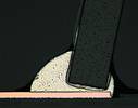
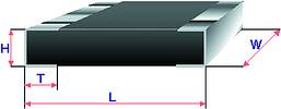
Tombstoning of passive chip components during the mass reflow soldering process has plagued circuit assemblers since the beginning of production SMT assembly. 'Tombstoning' - the partial or complete lifting of passive SMT components during reflow - is the phenomenon whereby small chip components, which are being soldered to SMT pads at opposite or polar ends, suddenly flip up vertically; sometimes the lifting is partial, and sometimes one sees them standing on one end like tombstones in a cemetery, on one of the pads (Figure 1). The mordant analogy is not lost on the circuit manufacturer; it is all too appropriate, since tombstoning means post-soldering rework and the death of a certain percentage of profits lost due to corrective action and higher per-piece costs to complete.
Early on in SMT, tombstoning was a problem usually associated with vapour phase (condensation) reflow, and was attributed to the rapid ramp-up rates characteristic of vapour phase heating, among other causes. With the decline in use of vapour phase technology, tombstoning all but disappeared, particularly with the advent of forced convection reflow technology and more sophisticated heating control.
However, tombstoning as a problem never went away completely, and has returned in greater incidence with the decreasing sizes and mass of chip components, as well as the use of higher-temperature lead-free solders. Tombstoning is most often encountered with greatest frequency when passive components become smaller; in vapour-phase reflow processes; in N2-reflow systems; and suddenly and unexpectedly with new batches of components and/or PCBs.
Probable causes
One cause of tombstoning is known to be differences in initial wetting of the solder, between both joints of a passive component. This disparity stems from differences in both the temperature and wettability of the surfaces of both joints. Ideally, both connections on either end of the component will reflow, wet, and form solder joints simultaneously. In this manner, the forces acting on the surface - wetting and solder surface tension, for example - will act in concert, cancelling one another out. When this does not happen, for example, should one end reflow and wet more quickly - the forces acting on that forming joint can lift the component up and on end before the solder on the other end has had the opportunity to melt and hold the end down through the strength of its own solder surface tension between the wetted end termination of the component and the wetted pad on the board.
What has wetting got to do with it?
The mechanism of wetting consists of three important parameters: 1) Time of initial wetting; 2) Wetting force; 3) Time of complete wetting. How soon complete wetting occurs has a direct bearing on tombstoning, because that is when the forces are greatest on the solder joint and the component.
If one end of the component reaches complete wetting significantly before the other side does, the wetting forces have the potential to 'pull' the component upright due to force exerted on the metallisation on the perpendicular edge of the component and top side if an overabundance of solder exists. This will lift the unreflowed end of the component up off the pad and out of the solder paste, causing the tombstoning phenomenon.
Thermal mass is a factor
The thermal mass of the solder joints at either end of the passive component have a direct effect on the cause of tombstoning. Unequal thermal masses of solder are a surefire recipe for tombstoning, since the lesser mass of solder will reflow sooner, wet sooner, and thus, exert physical force on the component sooner. Differences in the thermal mass of both solder joints of a passive component are caused by the following factors: tolerances in pad dimensions; tolerances in component metallisation; tolerances in the volume of printed solder paste; differences in heat dissipation through vias or inner layers.
Thermal mass of pads
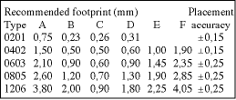
The larger the pad dimension, the greater the surface area of molten solder and the greater the effect of surface tension. There is great variation in pad dimensions because although there are recommended pad dimensions for specific component types, the tolerances are not specified. Varying tolerances can have a tremendous effect on pad mass.
Additionally, pad size and tolerances should be relative to placement accuracy. Too often they are not, and pad dimensions/mass are consequently disproportionately large relative to the component, contributing to tombstoning. These values are shown in the diagram and table of pad dimensions and recommended tolerances in (Figure 2).
Thermal mass of terminals
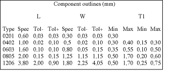
The varying thermal mass of terminals related to component types and outlines directly affects the rate of heating and time to reflow. Again, these tolerances are expressed as nominal values, but they should rather be relative because (naturally) the smaller the components get, the more important tolerances regarding dimensions become on pads, metallisations and also with regard to placement accuracy. These values are shown in the diagram and table of terminal types and component outlines in Figure 3.
Thermal mass of solder paste
Less solder paste will reflow more quickly than an excess deposit. No matter what type of application method is used - stencil printing, cartridge printing, or dispensing -the amount of paste deposited must be appropriate to form a good solder connection, and not excessive. More importantly, the amount must be uniform from pad to pad prior to reflow. 3D imaging of the paste deposit helps the process engineer monitor the thermal mass of the solder paste to keep it under control.
While a smaller thermal mass will heat up more rapidly, component position actually plays a role in rate of heating. For example, registration problems may cause significant displacement of the component terminals relative to the pads, causing disruption of thermal mass and resulting in larger ΔTs. The result is that the solder paste will melt a fraction of a second sooner.
A balancing act: minimising ΔT
The cleaner and more oxide-free the surface of the pad/terminal are, the lower the interfacial surface tension will be; the sooner initial wetting will occur; the stronger the wetting force will be; and ultimately, the sooner wetting will be completed. Consider that when surfaces in both joints are oxidised to the same degree, some oxidation will delay initial wetting. Delayed initial wetting provides more time for the temperature in the larger pad/terminal to rise, so that ΔT is minimised.
As a rule of thumb, the smaller the ΔT, the smaller the time differential of initial wetting.
When both terminals of a passive component do not have equivalent wettability, tombstoning can result, since the more solderable end will reach the complete wetting stage sooner.
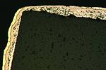
What factors can most commonly affect wettability? One example is when the metallisation of component terminals can become damaged, or are improperly plated or contaminated, reducing the wettable surface area. In (Figure 4), we see a microscopic image of a micro-section of a tombstoned resistor. The unsoldered and lifted side indicates that a part of the tin plating is missing, thus reducing solderability.
The role of N2 and vapour phase
Because N2 prevents re-oxidation of surfaces during ramp to reflow, it helps speed initial wetting. The vapour phase process should include a controlled ramp of temperature. In a scenario similar to that of an N2 environment, the vapour blanket prevents re-oxidation of surfaces during ramp to reflow. For both processes, this implies significantly less oxidation of metallic surfaces upon transit into the reflow phase when compared to reflow processes under ambient conditions. By consequence, these cleaner surfaces will wet faster. Fast initial wetting does not provide more time to reduce the ΔTs. The extra delay in initial wetting to reduce the ΔTs is exactly what is needed to minimise tombstoning. Therefore, in addition to the apparent benefits of both N2 and vapour phase soldering, extra precautions have to be taken to minimise tombstoning.
Two primary factors
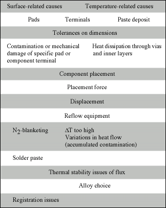
Table 1 illustrates that there are basically two types of causes of tombstoning; those related to surface of the PCB and components (such as solderability, oxidation, physical damage of plating, and those related to temperature (ΔT and heat dissipation. As Table 1 shows, there are areas where both causes have a combined effect, as in the choice of solder paste, where thermal stability issues and alloy choice must be considered in concert.
Solder paste solution
Eliminating tombstoning or at least greatly minimising it can be achieved in part through the solder paste recipe. First, use a solder paste with a thermally stable flux system that will maintain tackiness. Then, use a solder paste with metal particles with two different eutectic points: 50% melting at 179°C and the balance melting at 183°C - alloy after reflow: Sn62.5/Pb36.5/Ag1.0.
The angling effect caused by the wetting force in the joint that melts more quickly is mechanically hindered by solid particles of the alloy that melts at 183°C. This provides the alloy that melts at 179°C on the other pad with a fraction of a second more time to wet as well, thus restoring equilibrium.
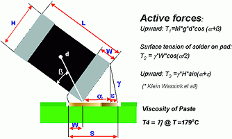
Klein Wassink1 initially described the phenomenon of tombstoning in a model in which forces of surface tension play a dominant role. The model, however, ignores the impact of the viscosity of the solder paste during melting.
In the temperature range of 179-183°C, the solder paste in fact has become a suspension of solid Sn63 powder particles in the liquid Sn62. This suspension evidently has a substantially higher viscosity than a solder paste that has become liquid entirely. This higher viscosity balances out the surface tension forces by mechanically hindering the angling effect of the component. Therefore, viscosity has been added as an important parameter to this model, which is shown in (Figure 5).
What is the solution?
In addition to using a solder paste with the abovementioned characteristics, tombstoning can in large part be prevented by following three rules of thumb:
1. Minimise ΔT in the board through control of the thermal (reflow) processing profile.
2. Control the tolerances on boards, components, and component placement.
3. Control the O2 ratio in N2 systems; preferred level is 500 ppm.
Tombstoning is a preventable defect; attention to its causes and addressing each of them will reduce its incidence, resulting in higher yields, lower defect rates, and less rework overall.
For more information contact local Cobar representative, Zetech, 011 789 3230.
Reference:
1. R.J. Klein Wassink, Soldering in Electronics, 'Drawbridging of Leadless Components', Electrochemical Publications, Isle of Man, Second edition, 1998,
pp. 609-616.
Harry Trip is product applications manager at Cobar Europe BV, Breda, Holland.
| Tel: | +27 11 609 1244 |
| Email: | [email protected] |
| www: | www.zetech.co.za |
| Articles: | More information and articles about ZETECH ONE |


© Technews Publishing (Pty) Ltd | All Rights Reserved
 printer friendly version