


The applications for BGA, FBGA, CSP and FlipChip interconnection techniques are expanding into broader fields of application. Since these substrate-based solder joints are scarcely accessible to other optical inspection methods, the use of non-destructive X-ray inspection is consequently on the rise.
Rather than investing in their own systems, many medium-sized firms and larger companies' QA departments opt to use external X-ray inspection service providers, who must therefore be capable of handling small to medium series of a high mix of products. They must also offer a wide range of inspection services, from standard quality control for commercial production, to the detailed analysis of potential failures. In order that they may perform this in an efficient way and produce reliable results, inspection service providers need objective, valid inspection methods and suitable X-ray systems. The biggest problem they currently face is the fact that evaluation and control software requires long set-up times - times which become unwieldy when the series to be inspected is small. Solutions to this problem include the use of semi-automated computer-controlled X-ray systems - this article looks at the results of this approach for these applications.
Test criteria and requirements
Functional integrity: When inspecting for the functional integrity of an assembly after the BGA soldering process, it is necessary to look for qualitative faults such as the following:
* Solder bridges (shorts).
* Missing solder joints.
* Misalignment.
* Open solder joints.
Bridges, missing joints and misalignment are easily recognised by the operator in an overview image. In contrast to these larger defects, open solder joints are more difficult to detect, normally requiring inspection to be carried out at higher magnification from an oblique angle. In this way it is possible to see either a gap in the solder joint or solder formed in a way that indicates insufficient wetting of the pad (in most cases the board pad).
Superior to laminographic (or planartomographic) methods, in terms of detection efficiency and time needed, this procedure has proved to be the best X-ray method possible for the detection of open joints as demonstrated by an independent study on 1,5 mm pitch PBGAs.
When inspecting smaller solder joints such as those in FBGAs, µBGAs, CSPs and Flip Chips, an oblique view seldom provides sufficient magnification, as the tilting of the sample under inspection takes the solder joints too far away from the X-ray source. Thus an X-ray system must be capable of ensuring high geometrical magnification even at angled inspection (OVHM: oblique view at highest magnification).
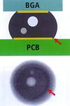
Reliability: other criteria must be taken into consideration when evaluating the reliability of an electronic assembly. First of all, the quality of the pad wetting is of interest, and here it is necessary to see whether the joining pad area is defined by a solder mask overlapping the pad or by the etched copper pad itself. In the first case, the joining pads appear as dark circular areas if they are well wetted. In the second case, well wetted pads are embedded in the solder and characteristic dark rings are visible in the X-ray image at the pads' edges, due to the additional solder in this area (Figure 1).
An oblique view at high magnification enables a more detailed investigation of the wetting status at the pads. Voids may compromise joint reliability, so it follows that the evaluation of a connection's reliability must also include inspection for voids, which show as bright circular areas inside the solder joints (Figure 1). The visualisation of these features places considerable demands on an X-ray system's capabilities. This is because solder joints absorb X-rays extremely well, while PCBs do not. Thus there is a fine line to be drawn between putting enough intensity into the joint to be able to see it, without causing saturation effects in the adjacent PCB, which can produce unwanted visual effects such as the apparent shrinkage in diameter of solder balls. This implies that in practice the X-ray system has to be operated at high tube voltage (120-130 kV), at low tube current (4-20 µA) and with a small focus spot size (<10 µm).
Quantifying test results
Going beyond the fundamental investigations into the dependence of solder joint quality on process parameters, reliability requires suitable control of the production process. This typically means the use of statistical methods, which in turn require that objective and well-defined parameters are measured quantitatively for as many samples as possible (up to 100%).
For example, a joint's reliability is not necessarily affected by the presence of voids - it is, rather, the amount of void area per solder joint area, normally stated as a percentage, that will affect reliability. This percentage is sensitive to process parameters, making it necessary to measure the relative void size for every individual solder joint. The test criteria which can be automatically evaluated during the inspection of production series are listed in Table 1. Any given BGA solder joint can now be evaluated simply by comparing a set of measurement data with threshold values, also making it possible to conduct semi-automated 100% sorting.
Case study - manual inspection with automated evaluation
Tests carried out on small series of assemblies involved moving the test sample under the X-ray beam manually, using a joystick. The joints were evaluated using dedicated BGA software. For standard BGA, FBGA and CSP solder joints the software was set up using the self-teach mode, and the system recognised the BGA layout, the right solder joint diameter and the grey level directly during the evaluation process without requiring additional set-up time. The system measured all of the criteria shown in Table 1 against pre-set threshold values.
Thanks to an auto-set-up function, the operator did not have to monitor positioning and magnification during manual inspection, which saved time, and the results were independent of variables in X-ray parameters as long as they were kept within a certain range. The auto-set-up worked properly as long as at least about 80% of the solder joints in the field of view met the acceptance criteria for diameter and grey level, which was the case for most applications.
Where this was not the case, target values were learned from a group of acceptable solder joints or typed in directly while the program assisted with estimate values and measurement tools. Typical set-up time here was about 10 minutes for one component type while time overhead for evaluation is about 2 seconds. This means that total test time is mainly determined by manual manipulation.
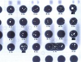
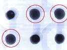
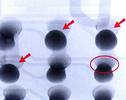
The automated evaluation of a standard PBGA 255 including 4-6 views requires a maximum of 1 or 2 minutes. Figure 2 shows the result of a BGA series inspection. Here, maximum void acceptance was 5%. It should be noted that the background structures (solder on the other side of the PCB), although clearly visible, are suppressed during evaluation and do not influence the test result. In this case, abnormal solder joints had to be inspected both under high inspection and in the OVHM mode in order to understand the defect mechanism. Figure 3, for example, shows 6 solder joints on a µBGA component - it is easy to see the slight misalignment and irregular solder joint diameters. Wetting defects have been identified according to the above-mentioned criteria (no dark ring, missing plateau) in the joints that are marked. In the OVHM image (Figure 4) these solder joints turned out to be actually open - the solder is only attached to the component pads. The lower left solder joint shows the central plateau in top-down view. In the OVHM image, however, it is also shown to be open, due to the missing solder meniscus.
Automated offline inspection
For bigger sets of samples it makes sense to use automated offline inspection. Here, samples are moved by autopositioning and the solder joints in the field of view are evaluated automatically, after which the test results are saved in a record file.
The test programs for components with standard layout (full rows of joints) can use the BGA evaluation software auto set-up: just the test positions must be accessed and taught in manually. Layouts that deviate from standard (eg, single unused connection positions) can be entered by means of a graphical menu for each view individually. The same applies to the threshold values and, if necessary, other parameters including X-ray parameters. In this way, different BGA components mounted on the same board can be inspected in one cycle.
In practice, the set-up time ranged from 5-10 minutes for a µBGA to 5-30 minutes for a BGA with several hundred solder joints. The time for an inspection cycle including all criteria in Table 1 ranged from several seconds (µBGA with two views) to 2 minutes (BGA 352 with 40 views).
Conclusion
The applications performed until now demonstrate that, thanks to minimised set-up times, automated and quantitative testing of substrate-based solder joints is feasible and worthwhile. The OVHM technique now enables the analysis of finer pitch (CSP, FlipChip) solder joints at high magnification in oblique views. An automated evaluation of oblique view images and of the wetting criteria mentioned above would be desirable. This, however, would require an extended approach to image analysis algorithms because of the variety of the defect indicating features.
| Tel: | +27 11 609 1244 |
| Email: | [email protected] |
| www: | www.zetech.co.za |
| Articles: | More information and articles about ZETECH ONE |


© Technews Publishing (Pty) Ltd | All Rights Reserved
 printer friendly version