


New high-speed architectures require a closer view on the complete signal path. Elma TreNew Electronic's new HiSpeed Test System helps determine the influence of the interconnection elements.
Problem: Bus structures like PCI (peripheral component interconnect) or VME (VERSA module Eurocard) were developed in the last decades. The data transfer of these multipoint bus structures are limited by the CPU clock frequency, bus protocol (eg, 'VME Handshake') or the number of data lines. For example the bandwidth of a cPCI backplane is limited to 533 MBps (64 bit @ 66 MHz), but the needs of today's applications are orders of magnitudes away from this. Higher bandwidth requires other solutions, for the chipsets on the cards and the protocols, but also, for connectors and the backplane topology!
Because of that, groups like PICMG (PCI Industrial Computer Manufacturers Group) and VITA (VMEbus International Trade Association) are defining new specifications that supports the newest technologies and architectures in high-speed data transfer and bandwidth requirements:
PICMG 2.16: CPCI packet switching backplane
PICMG 2.17: StarFabric PICMG 2.20 CPCI serial mesh backplane
PICMG 3.x: AdvancedTCA
VITA 31: Gigabit Ethernet on VME64x
VITA 34: APS - advanced packaging system VITA 4 VXS VMEbus switched serial standard
Some of these new specifications are already released, some are still in work.
Solution
Most of these new specifications use a common way of increasing the bandwidth for applications with a need of high data transfer rates. The solution is to use 'point-to-point connections' transferring packet switched data via differential pairs with a speed up to 3,125 Gbps. The near future will allow data transmission of up to 5 Gbps, and with 10 Gbps close to come. At such speeds the quality of the signal is negatively affected by several factors on its way from transmitter to its receiver. Therefore, the design of such high-speed backplanes requires also a new thinking. To guarantee functionality and reliability it is mandatory to see the complete signal path (card - connectors - backplane - connectors - card) as one entity.
To investigate this new approach, Elma Trenew designed a High-Speed Test System (backplane plus cards) to determine the influence of the interconnection elements like connectors ('HiSpeed connectors'), material, trace width and length ('dielectrical losses' and 'skin effect'), backplane thickness and vias ('stub effect'), and connector-based cross-talk.
All these parameters are essential for the signal integrity and have to be controlled by the designer of the backplane. Furthermore, all parameters are related one to each other, so that - at high speeds - a change of only one of these elements implies a new adjustment of all the others. To be able to determine the influence of each interconnection element, the test backplane is divided into three different sections:
* Reference area (SMA coaxial contacts, 50 Ω): allows to determine only the influence of backplane traces without any influence of the HiSpeed connectors. Differential lines edge coupled/broadside coupled, and single ended lines are implemented with different trace widths in different layers.
* Link area: consists of real interconnection paths. Edge coupled, broadside coupled differential lines and single ended lines with different trace widths and trace length situated in different layers can be investigated. Four HiSpeed - differential - connectors (the most representative on the market) are present, plus additionally the HM 2,0 mm connector (standard CPCI).
* X-talk area: allows to investigate the amount of cross-talk introduced by the connectors. A total amount of 555 differential links and 80 single ended lines are implemented in the backplane, allowing various measurements to be performed, in order to see the influence of only one interconnection element and the influence of combinations of these elements.
For example, by comparing traces with the identical topology situated in the same layer but with different lengths can be observed only the influence of the trace length. In the similar manner, by comparing traces situated in the same layer with identical lengths but routed with different widths can be observed the influence of skin effect only. The 'stub effect' can be analysed by measuring similar links but located in different layers.
For completion of the signal path, (passive) test cards were designed for all connector types used on that backplane. All these cards were made in FR4, impedance-controlled, and all the traces were routed with the same width and length to have the same influence on the signal. SMA coaxial contacts, in total about 1000 for all cards, give the possibility to perform measurements for various topologies.
Two measurement methods were performed, one by using real drivers (up to 3,125 Gbps), the other by using a data pattern generator (up to 10 Gbps) on the transmitting side, and a signal analyser to investigate the received signal.
Summary
Here follows a short overview showing the influence of each interconnection element:
The signal speed or data rate is the most important factor because the losses and also the cross-talk increase with the frequency but in a different manner (for example dielectric losses are related directly to the frequency, and skin effect to the square root of frequency).
The drivers or chipsets used to transmit data have a big impact on the signal quality. On the market many drivers are present for different speeds with a different behaviour, with or without built-in terminations, with or without selectable pre-emphasis levels, that need to be AC or DC coupled and so on. However, a backplane shall be 'driver agnostic' and to achieve that, it is very important to know the behaviour of different drivers. Simulations were made to analyse the signal integrity on the backplane, with different types of drivers.
Trace width is an important factor for high-speed signals. It is commonly believed that the wider the traces, the better the signal integrity, because wider traces result in lower skin-effect losses. This is correct, however, but few aspects need to be considered when using wide lines: First, wider traces result in lower signal-routing density which can lead to more signal layers. Wider traces also require thicker cores and prepregs, in order to achieve the desired impedance, resulting in thicker PCBs. So, the desire for wider traces to reduce skin-effect losses can result in thicker boards with more layers, which will increase the critical 'stub effect' (see also below).
Trace length is another important parameter besides trace width and board thickness for finding the best design compromise, because the losses due to skin effect and also the losses in dielectric material increase with trace length. So, it is possible that the best compromise between trace width and backplane thickness for a certain length may not any more be the best solution for the longer trace (because the stub influence remains constant but the skin effect is increased). It is possible to find another compromise, increasing the stub effect a little and minimising the skin effect, to get smaller total losses. In consequence, measurements and simulations were performed for different trace widths and trace lengths, to determine at which frequency and data rate the trace width starts to make enough of a difference.
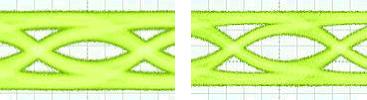
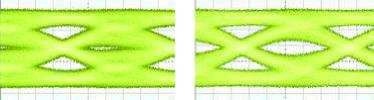
To highlight the described behaviour of different trace width and length there are two pairs of eye diagrams as shown in Figure 2a and b. Figure 2 presents the results for two links routed with different trace widths 5 mil (case a.) and 8 mil (case b.). The measurement was made at 10 Gbps. The 8 mil case means an improved eye opening with 37% compared to the 5mil case.
The results for two traces with identical width (8 mil), but length of 150 mm (case a.) and 400 mm (case b.) at a speed of 3,125 Gbps are shown in Figure 3.
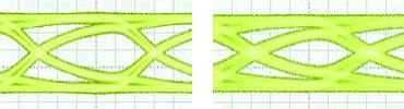
The pictures show very clearly a dramatic reduction of the eye opening (due to increased losses) at a speed of 'only' 3,125 Gbps.
Stub effect is denoted as the resonant effect created when the signal trace enters a hole on a top layer of the board and exits the hole on an internal layer, leaving an 'unused rest of' the plated through hole (Figure 4) that acts like a high frequency filter and creates an effective decrease in the impedance. Therefore, the backplane thickness is important because it determines the amount of the plated- through-hole stub that remains between the signal inner layer and the external bottom layer of the PCB.
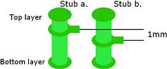
The stub length with respect to the optimised thickness of the backplane is a very important design parameter that, if ignored, can have an adverse effect on signal performance. This can be observed in Figure 5, showing the eye diagrams for two 10 Gbps links, identical from the topology point of view, but situated in different layers, with only 1 mm difference in their stub length.
It will be noticed that only 1 mm less of stub copper means a huge positive impact on the transmitted signal.
Cross-talk: Beside dielectric losses, skin and stub effect, higher frequencies increase also the sensitivity for cross-talk. To define the global solution (backplane thickness, trace width, trace length and connector type), the cross-talk shall be considered, too. Cross-talk can be minimised using thinner cores and prepregs to reduce the distance signal-to-ground (positive impact on backplane thickness) or by increasing the separation between differential pairs, but this is possible - in many cases - only by adding more signal layers (increased backplane thickness) or reducing the trace width (increased skin effect).
The connector type has a great impact on cross-talk level for two reasons. Firstly because cross-talk exists inside the connector and must be considered when calculating the total cross-talk, and secondly because in many cases the distance between differential pairs is imposed by the distance between the connector pins. Therefore, it is very important to know the specific connector influence: a special cross-talk section was implemented in the test backplane to verify only the cross-talk influence for all implemented connector types.
Conclusion
The design of backplanes for the new high speed architectures requires a lot of know-how and experience to find the best design compromises for stub effect, skin effect, dielectric losses, cross-talk, differential pair routing and matching of impedances. Before specifying the final requirements of a high-speed backplane (application) a close cooperation between customer and backplane designer is necessary to guarantee the signal integrity and the successful performance of the application. Only the cooperation with an experienced partner (simulation, design, production and measurement in one hand) leads to a good quality of the complete signal path.
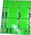
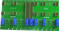
An example of an Elma backplane for such new HiSpeed architectures is shown in Figure 6. It is compliant with PICMG 3.0 (draft) 'AdvancedTCA', having 14 slots with 12 node slots and two fabric centred in the middle for two reasons: firstly to reduce the trace length to decrease the dielectrical and skin effect losses dramatically (up to 50%); secondly, to apply an optimised routing strategy that leads to the best layer number possible - only 12 layers has had a large positive impact on the signal performance (thin PCB minimises stub effect) and more effective cost saving. Only deep design experience and know-how can lead to such benefits for the customer in performance and costs.
Elma TreNew Electronic is represented in South Africa by Systematic Designs, 021 555 3866.


© Technews Publishing (Pty) Ltd | All Rights Reserved
 printer friendly version