According to the thermionic emission model, pure Schottky barriers exhibit a forward voltage drop, which decreases linearly as the barrier height diminishes; whereas the reverse current increases exponentially as the barrier height decreases. Consequently, there exists an optimum barrier height, which can minimise the sum of forward and reverse power dissipation for a particular application. However, users of Schottky diodes have revealed that they do not search for minimum forward and reverse power dissipations, but always for the minimum forward voltage drop. Reverse current values are very rarely asked for. One must know how the Schottky diode is being applied in order to objectively select the most appropriate part.
In high power applications with low circuit voltages and using Schottky diodes with blocking voltages less than 25 V, the forward power losses of the diodes still dominate in the balance of power losses. Prevailing applications are in switched mode power supplies. Here, it is argued that a 4 mV decrease of the forward voltage drop results in a reduction of the forward power losses of approximately 1%. Therefore, the components created for this application have low barrier heights (less than 0,74 eV) and highly doped, thin epitaxial drift layers. This results in a device with a low forward voltage drop and high but still acceptable reverse current.
On the other hand, in high power applications using medium or high voltage Schottky types (VRRM ranging from 45 to 150 V) the reverse power losses are comparable or can be even higher than the forward power losses. Nevertheless, most users do not ask for low reverse currents but again for only a low forward voltage drop.
Diode with an ideal dynamic behaviour
In addition to forward and reverse power losses, there is apparently a third quality, but one that is difficult to quantify. Nevertheless it has an impact on forward voltage drop as shown by experience. Supposedly this quality is exhibited by the dynamic properties and switching loss of the real Schottky diode. Due to their short appearance in the range of only a few nanoseconds, they can only be measured with costly test equipment and moreover, the slight differences in their dependencies cannot be made evident. With regard to the dynamic properties, the Schottky diode is generally considered as an ideal diode with a junction capacitance connected in parallel. Concerning the switching characteristics, the ideal diode is a pure majority-carrier component (only electrons in the n-region). After the zero crossing of the current from the forward state to the reverse state, the ideal diode fully ignores the previous conductive state and blocks reverse voltage immediately after the current crosses zero.
Fast reverse recovery pn-diodes
In contrast to the ideal diode, pn-diodes with minority-carrier current components still 'remember' their previous on-state after forward current has decreased to zero. This is due to the injected minority carriers (holes in the n-region), which will decay exponentially with an adjusted minority carrier lifetime t or are swept out by the reverse current. The pn-diode regains its reverse blocking capability with a delay after zero crossing of current. The minority carrier lifetime can be decreased by diffusing lifetime killers (gold or platinum) into the n-region or by exposing the diode chip to radiation.
Real Schottky diodes
Real Schottky diodes also have minority-carrier injection through their barriers, although it is smaller by several orders of magnitude. This phenomenon is called modulation of the epitaxial layer. The injection increases as the barrier height, voltage type, forward current density and the junction temperature increase.

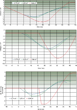
Due to the previously-mentioned technical measuring difficulties, we simulate the switch-off behaviour of real Schottky diodes. In Figure 1, the resulting current and voltage waveforms for a Schottky diode with a type voltage of 100 V and an active area of 0,323 cm2 are plotted versus time. The preset operating conditions are 50 A forward current, 300 A/µs during commutation, 25 V reverse bias voltage and 25°C junction temperature. Three different materials with barrier heights of 0,74, 0,8 and 0,86 eV are considered. The turn-off energies are 0,86, 1,0 and 2,3 µWs respectively. The simulation model clearly shows that the remaining minority carriers from the conduction phase in the n-doped epitaxial layer determine the initial conditions for the general solution of the differential equation of the LC circuit, which consists of a switch-off inductive coil, the junction capacitance and the forcing reverse voltage bias of 25 V. Due to the delayed capability of the real Schottky diode to block reverse voltage after commutation - growing with increasing barrier height, the resonant circuit reacts with an excessive reverse current (ie greater than the commutation switching-off slope multiplied by the square root of LC), an excessive reverse voltage (ie more than twice the driving reverse voltage) and a steeply starting, excessive dv/dt (ie more than the driving reverse voltage divided by the square root of LC). The excess of the dynamic parameters and switching loss becomes more evident as the barrier height is increased.
The reaction at a barrier height of 0,74 eV with respect to dynamic behaviour and switching loss is almost ideal for the example chosen above. Thus, having the abovementioned rule in mind - the lower the barrier the lower the forward voltage drop of pure Schottky barrier - shows that the search for minimum forward voltage drop not only diminishes forward power loss but also switching loss in real Schottky diodes. It explains the demand for low forward voltage drop even with high reverse current.

But this simple rule that low forward voltage drop corresponds to low switching loss does not hold for real Schottkys of type voltage above approximately 80 V. We have to take into account that forward voltage drop is the sum of drops over the actual barrier and the epitaxial drift layer. The second term becomes more pronounced with respect to the first term with increasing type voltage.
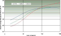
On the other hand, for increasing barrier heights and type voltage, the increased modulation in the epitaxial layer lowers the resistivity of and the forward voltage drop over the epitaxial drift layer. This lowering can become more pronounced than the increase of voltage drop over the actual barrier as Figure 2 indicates. Numbers for our 100 V example at 232 A/cm2 and room temperature are:
* Diodes with the lowest forward voltage drop of 0,78 V for highest barrier 0,86 eV have worst dynamic values.
* Highest 0,8 V forward drop for lowest barrier 0,74 eV have best dynamic values.
Thus, real Schottky diodes of type voltage above 80 V with lowest forward voltage drop are not the fastest.
Application-specific adjustment of barrier height
I am of the opinion that, for the circuit designer, deviations in the dynamic behaviour and the corresponding switching loss from the ideal diode with a junction capacitance represent more disadvantageous behaviour than a very high reverse current. In fact, the reverse current of a diode with a barrier height of 0,74 eV is about 25 times higher than that of a diode with 0,86 eV. Above a certain limit, the exponentially increasing reverse currents, typical of low barrier heights, become unacceptable. However, this depends on the respective application.
The objective at IXYS is to meet the special application requirements and the customers' needs by offering components with mixed barriers (values between 0,66 and 0,86 eV).
For further information contact Avnet Kopp, (011) 444 2333, [email protected] or www.avnet.co.za

© Technews Publishing (Pty) Ltd | All Rights Reserved