
In the fields of electrical and electronic engineering the word ground is used to describe parts of systems or PCBs (printed circuit boards). The reason for using this word is to denote some part of a system or structure that is ‘neutral’ or zero potential.
To the newcomer to the field it can be confusing trying to understand how so many things can be called by the same name.
Recently, there has been a lively discussion on one of the open technical discussion venues about the various kinds of grounds and methods for connecting them together. The kinds of grounds mentioned in the discussion include:
• Digital logic ground.
• Analog ground.
• Chassis ground.
• Safety ground.
• Earth ground.
Methods proposed for connecting these various ‘grounds’ cover a broad range of options including:
• Connecting them at only one point
• Cutting the ground plane under a mixed-signal component
• Connecting them with capacitors
• Segmenting the ground plane in a PCB such that there is only a narrow connection at one place between the analog and digital sides of the design
• Separating the analog and digital grounds
These seemingly conflicting methods for dealing with ground can be a bit confusing. Some clarification about what ground is would be a good place to start. Once this has been established, dealing with the above points will become clearer.
The first question that one might ask is: How can all of the items above be ground? The answer to the question is very straightforward. None of them are. Ground is the one place in an electronic system that is a reference point from which voltages will be measured.
What are these other things that are being called ground? Below is a short explanation of them.

Digital logic ground is the ‘reference’ terminal of a digital logic power supply. For most digital logic systems it is the negative terminal of the logic power supply. It is usually designated with the symbol in Figure 1.

Analog ground is the reference terminal of the supply that powers an analog circuit. It is where one side of an analog signal source is tied. The other side of the signal source is tied to the analog input or output. Analog ground is usually designated with the symbol in Figure 2.
Chassis ground is the name given to the connection of the safety wire from the AC mains to the case of a product. It gets this name because the case of a product is often called the chassis. This wire is usually the green wire in an extension cord, in the three-wire mains connecting to a product or the third pin on an AC connector (the round one).
If one traces this green wire through a building it will finally connect to a copper stake driven into the earth. The purpose of this connection is to protect the operator of the product in the event that one of the mains wires accidentally makes a connection to the case or chassis of the product. So, it is a safety-only function.

Sometimes, EMI gurus erroneously refer to this ‘chassis ground’ as a place that has some function in the containment of EMI. This statement never has or never will be based on fact because it has no role in this part of an electronic design. Chassis ground is usually represented by the symbol in Figure 3.
Safety ground is another name used to describe chassis ground.
Earth ground is another name for the safety ground.
This leads to the question of how to connect all of these ‘ground’ circuits together or whether they should be tied together in the first place and, if so, why. This question usually arises for one of two reasons: either the discussion centres on how to protect sensitive analog signals from outside noise sources or how to contain EMI.
Handling analog signals
Taking the analog signal problem first, the engineering objective is to protect the analog signal from sources of outside noise that could degrade signal performance. Figure 4 is an example of a typical mixed analog and digital integrated circuit showing the two sides of the circuit and both an analog ground pin and a digital ground pin on the IC. It is representative of most of the problems that are of concern when designing mixed-signal electronics.
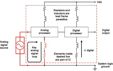
Highlighted in red is what is called the analog decision making loop. This is the circuit that must be protected from outside noise sources in order for the circuit to perform properly. First, the reason there is an analog ‘ground’ pin and a digital ’ground’ pin on the IC needs to be understood in order to arrive at a proper PCB design.
The digital side of this mixed-signal IC has transient currents flowing through its ground lead that are associated with the internal digital processing of the analog signal as well as for driving the output transmission lines. If this were an 8-bit analog-to-digital converter (ADC) in a logic system with 2,5 V logic levels, the current transients flowing in this path could be as large as 200 mA. This I or rapidly changing current flowing through the ground lead inductance can develop voltage transients as large as 100 mV between ground on the PCB and ground on the die. This is an acceptable transient as far as the logic circuit is concerned.
If the circuit under discussion is a 12-bit ADC, the analog side of the circuit is tasked with resolving voltage differences of 0,5 mV out of a total signal swing of 2 V. If there is only one ground path out of the IC, the 100 mV digital switching transient would be superimposed on the analog signal, rendering the circuit useless. This is the reason that the analog side of the IC has a separate ground path out of the package.
Figure 4 is typical of circuits that have application notes or other guidelines that specify having an analog ground plane and a digital ground plane or splitting the ground plane under the component. Doing either of these things detracts from the actual engineering problem, which is protecting the analog signal loop from external noise. (Note: The direction of the current flow arrow in Figure 4 is the flow of the electrons which make up the current flow.)
If a designer chooses to split the ground plane under the component an unwanted side effect is created. This side effect is that signals that must cross from one side of the cut to the other do not have a path for their return current which can lead to signal integrity or EMI problems.
How does noise enter the analog signal loop? There are two ways this can happen. The first is by coupling into either side of the loop by capacitive coupling or magnetic coupling from an adjacent signal travelling too close. We usually call this crosstalk. Crosstalk can be generated by the electric component of the electromagnetic (EM) field (called capacitive crosstalk) or the magnetic component of the EM field (called inductive crosstalk). Which form exists depends on the configuration of the two conductors that are next to each other.
The second case of noise is by allowing the ‘ground’ side of the analog path to be shared by another signal. This usually happens when the connection between the analog source and the analog ‘ground’ pin of the device is made to the ground plane some distance away from the part.
In most cases, both of these problems are addressed by using a shielded cable that has its two connections made at the terminals of the IC, one connection being the shield that connects to the ‘analog ground’ terminal of the device and the centre conductor that connects to the input side of the analog device.
Examples of this type of circuit are the connection between the read head on a disc drive and the preamplifier; the connection between a strain gage and the input amplifier; the connection between a phonograph needle and the input preamplifier (only old guys know about this!).
The example in Figure 4 deals with a system where the analog source is ‘off board’. When both the source and load are on the same PCB, the proper way of dealing with the ‘analog loop’ is to look at where it is and make layout choices that protect the loop from crosstalk and voltage gradients in the ‘ground’ part of the circuit that would compromise performance.
In almost all cases, this problem is dealt with by choosing to carefully place the components on the PCB surface so that no currents from other circuits flow through the region where the analog decision making loop is located. Examples of this type of circuit are connections between amplifier stages in a radio; and connections between amplifier stages in a stereo system.
Handling EMI
Sometimes I find it useful to quote a fellow EMI engineer, Bruce Archambeault, when the subject of ground comes up in relation to EMI: “Ground is a place where one sows seeds in hope of reaping a bumper crop of tomatoes come summertime.”
The reason that both Bruce and I make this statement is that using the word ‘ground’ in discussions about EMI has no value. In fact, it distracts us from the task at hand, which is containing RF energy that might escape our products and create an EMI failure.
Said another way, none of the things listed as grounds at the beginning of this article have any bearing on EMI containment. The items that are important to EMI containment are shields on cables and Faraday cages surrounding the products, but that is the subject of another article.
What is a Faraday cage?
Throughout this article I have used the term Faraday cage when discussing EMI issues. It might be helpful to explain what a Faraday cage is and what it does.
A Faraday cage is a metallic enclosure it which an electronic product such as a computer is housed. Its purpose is to contain energy that has escaped from the product in the form of electromagnetic waves and could create an EMI problem if allowed to find its way to a nearby product. An example of a Faraday cage is the enclosure that houses a router or switch.
The Faraday cage is often made up of the side panels of a card cage, the backplane and the faceplates of the plug-in modules. This is probably why some call it ‘chassis ground’ – it just so happens that part of the Faraday cage is made up of some or all of the material that also forms the chassis of the product.
When signals and power cables penetrate the Faraday cage the possibility of EMI escaping on those cables is created. In order to prevent this, shields are placed around cables that contain frequencies that are in the EMI frequency band. So, shields are extensions of the Faraday cage as long as they are attached with a very low-impedance connection.
For wires that cannot be shielded, such as power cables and mouse connections, some form of RF filtering must be placed on those wires as they exit the Faraday cage to prevent them from causing an EMI problem. An example of this is the ferrite toroids that are placed on power cords as they exit a box.
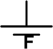
Figure 5 is the symbol I have created to indicate where a connection is to be made to the Faraday cage.
Summarising
There is a very large body of misinformation in print in the form of application notes and guidelines with respect to what ground is and how to use it. Some of the applications notes I refer to indicate that the ground plane should be segmented into an analog side and a digital side, and the two sides connected at only one point. Others suggest that there be two discretely different planes, one analog and the other digital. How these two planes are to be connected varies with each application note.
My experience with these notes is that they are treating a problem that has not been proven to exist. The worst thing about such notes is that they do not address the actual problem that needs to be solved. That problem is protecting the decision-making loop from outside noise sources.
One criterion that should be applied to any of these rules is, is whether there is proof that a real problem exists, that the proposed solution solves the problem, and that the proposed solution does not create a new problem such as an EMI problem.
If these three questions do not have valid answers, chances are the solution is simply made up and may well create a problem, such as an EMI problem, that might otherwise not exist. Many EMI problems I have solved have had their origins in split ground planes. The most common place I saw this was small disk drives in the late 1990s and early 2000s.
Electronic systems have networks we call ground that must be understood to have both AC and DC voltage gradients in them as a result of currents that flow, so they cannot be considered equipotential with magic properties with respect to EMI.
A PCB does not need an analog ground plane and a digital ground plane as that does not guarantee proper operation of the analog section of the product. Instead, it should have only one ground plane that should be continuous throughout the PCB, followed by careful design of the decision making loop.
Splitting a ground plane destroys its integrity as an ultra low-impedance connection between all of the components in a circuit and should never be done. I have asked more than 9000 students in my signal integrity classes if they have examples where splitting a ground plane improved performance. To date, none have been able to produce one, nor have any of my engineering colleagues.
In those rare cases where the ground plane must be split for high-voltage isolation purposes, signals that must cross the split will need to do so in such a manner that the need for a continuous return current path is not required. Two ways this is done is with transformer coupling, which does not work for signals that have a DC component, or by using optical isolators.
The thing called ‘chassis ground’ is a safety-only feature and has no role in the electronic function of the circuits or their EMI performance. It is not necessary to connect logic ground to the ‘chassis ground’ and, in some instances, it is not allowed. An example of this is a system that contains an RS-232 interface that does not allow connection of logic or signal ground to the case which is connected to the earth ground.
Perhaps one of the toughest challenges a design engineer faces is sorting through all of the misinformation in print and online that is inaccurate or, often, simply made up by someone who has not done the necessary research to ensure the advice given is technically valid.
Hopefully, this article can serve as a good starting point for demystifying the things that are erroneously referred to as ‘ground’ in the PCB design industry.
| Tel: | +27 12 665 0375 |
| Email: | [email protected] |
| www: | www.edatech.co.za |
| Articles: | More information and articles about EDA Technologies |
© Technews Publishing (Pty) Ltd | All Rights Reserved