


With 3D solder paste inspection (SPI) becoming more and more established and offered by multiple suppliers, it is often assumed that this is the final stage in solder paste inspection. A closer look as to what 3D-only systems can and, importantly, cannot detect, shows that there is room for further yield improvement.
By looking at the traditional characteristics of advanced 3D and 2D imaging, strengths of both can be utilised, especially if combined within the same measurement cycle. With the introduction of ‘5D’ SPI, all types of print process errors can be reliably identified and prevented.
Two dimensions (X and Y) are needed to measure area parameters such as offset, smearing, shape and bridging. The third dimension (Z) adds additional height and volume information. Combining the best techniques to identify anomalies in each axis clearly improves the return on investment (ROI) for SPI equipment, and enables a new generation of closed loop process control.
Post print SPI
Many process engineers and quality managers still question the value of solder paste inspection. Although it has been agreed for years that high percentages of end-of-line defects can be traced back to the print process, SPI has not been deployed in a significant percentage of SMT lines.
Many still question the ROI analysis. Others consider the need for SPI critical during the new product introduction phase or production ramp-ups, but not beneficial for mature, established processes. For them, the information provided by the SPI does not bring any relevant product quality improvements, or they perhaps are unable to usefully apply the improvements.
Nonetheless, research done at IBM in Austin almost two decades ago clearly identified solder paste volume as the most important characteristic contributing to good solder joints.
Unlike the ‘random number generators’ (to quote the late Dr Steve Case, a pioneer in 3D SPI) that no doubt impacted the attitudes of many production engineers, today’s technologies can provide reliable volumetric data as well as crucially important X-Y data.
Structural test verification technology clearly identifies the value of adding SPI, and while typically the need for in-line solder paste inspection is driven by maintaining production line stability and providing notification of process deviation, frequent changeover and smaller run sizes demand special performance capabilities to properly serve such manufacturing environments.
These include:
* Printer verification, even on first time builds.
* 30 minute or less CAM to board test time.
* Minimal false calls.
* Data with traceability to downstream inspection and test.
Modern manufacturing trends are increasingly abandoning repairs in favour of prevention through improved process control. This is particularly the case in automotive electronics. The typical printing problems causing end-of-line defects can be detected by SPI and therefore offer significant opportunity for permanent yield improvement and reduced cost to manufacture.

2D techniques
In the first automated SPI applications, conventional AOI machines were used to verify correctness of the solder paste deposit after print. Specially developed algorithms were able to measure important 2D parameters such as coverage, offset, shape, smearing, slumping and bridging of the paste by using the stencil’s Gerber data as programming input file.
Defects from those parameters can all be detected by a 2D analysis in combination with tolerances set onto the Gerber reference.
Later the 2D SPI inspection evolved to better algorithms and better capturing systems. The use of RGB lighting systems in combination with different lighting angles dramatically improved the detection capabilities by isolating the solder paste from any type of PCB background, such as PCB colour, copper, gold, solder resist, silkscreen, tracks and vias.
After isolation of solder paste is successful, reliable 2D measurements can be obtained. 2D inspection methodologies are line scanning (line sensor) in greyscale or colour or area scanning (field sensor) in greyscale or colour.
Using 2D technology, two parameters cannot be obtained: height and volume of the solder paste deposit. 3D technology is needed to capture these parameters.
The additional benefit of 3D versus 2D is often questioned, as 2D will capture most of the defects appearing in the printing process. On the other hand, what could be the added value to measure 3D parameters such as height and volume?
3D techniques
Laser triangulation and phase shift Moiré are the most commonly utilised techniques to measure solder paste height in 3D SPI, and both methods have strengths and weaknesses.


Common for both methods is to measure only the height of the deposit. By integration of the height data of each XY pixel the corresponding area and volume data is calculated.
To obtain accurate height data of the deposit, which is typically between 50 µm and 300 µm in a normal printing process, it is crucial to measure the height from the correct reference. This zero reference is typically the surface of the pad onto where the paste is printed.
Because the solder paste is covering the pad after printing, the pad surface cannot be used as reference for the height measurement. To create a decent accuracy, the pad surrounding is usually used as zero reference and this also compensates for inevitable board warp.
If the board warp is significant, and the pads are not horizontal, the zero reference can be obtained by applying a 3D reference plane over the pad to be measured, that follows the board warp.
By using the surrounding of the pad for zero referencing, a correction has to be applied, because the surrounding of the pad has a height offset compared to the pad surface. To obtain this height offset, usually a golden board is used to capture the offset data of each pad.
The use of a golden board in the programming stage to obtain height offsets only gives accurate results if the production boards are identical to the golden board (same batch) and different surface layers onto the PCB are not varying in thickness (stable PCB manufacturing process). In reality both are rather uncommon.
Laser triangulation is amongst the oldest technologies used to measure height of solder paste deposits. The laser projects a top-down laser slit beam and a camera is used to capture the reflected laser lines. The laser head is moved in defined pitches to cover the target area and the triangulation method is used to calculate the height.
To obtain better repeatability, two lasers can be used in a 180 degree setup. The height data from both measurements is averaged to reduce the effect of the deposit shadowing itself near steep edges.
Moiré topography is a method of tri-dimensional measurement by phase modulation. In the Moiré method, lines are projected on an object as modulated interference fringes, and by moving the observation grating which creates the lines, the height of the object can be measured.
The grated light is projected on a target and the resulting image is captured at known angles, using an area scan sensor and its height calculated with basic triangulation mathematics.
Inspection of a large area is done by merging a sequence of small area scans (the sensor’s field of view or FOV), sometimes with an optional Z-adjustment for focus to compensate for board warp. The method becomes repeatable by incorporating oversampling techniques.
At the same time, variations due to colour and reflection changes are reduced through the use of a white light source. However, the range of measurable height is narrow and particularly inconsistent at low heights (ie, below 50 μm).
Near the merge of two FOVs, covering the same area (eg, the print of a large BGA type), the focal references and optical distortion can vary and result in differences in height or volume measurements. This in turn can produce inaccurate indications of solder paste quality, even when measurement results are very repeatable.
Board warp further complicates the measurements and usually degrades accuracy and repeatability figures.
Dual multisampling laser systems combine the advantages of Moiré systems and laser. Dual multi-angle colour lasers can accommodate different PCB colours and eliminate the shadow effects at the same time. The multi-sampling technology of doing multiple measurements on each object detail boosts resolution, accuracy and repeatability figures while maintaining fast speed of a scanning laser and XY accuracy.

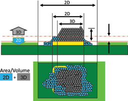
Where 2D inspection detects nearly all possible defects, 3D inspection gives quantifiable volumetric data. This volumetric data can be used for process control in order to adjust printing parameters and settings before defects occur.
In Figure 4, an example is given of multiple inspections on a specific aperture size. The area and volume data are compared - if the relation between volume and area was linear, the result would be represented by the 1:1 line. In this graph the deposit volumes vary by more than 50% for the same area. This could occur if not all deposit leaves the apertures while releasing the stencil.
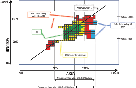
On the other hand, for the same volume, the area spread is up to 65% for equal volume. This could occur if paste slumps underneath the stencil and could lead to bridging or poor wetting. For tight process control, both area and volumetric data have to be monitored carefully.
The introduction of 5D SPI
A brand new approach to SPI enhances the benefits of 3D imaging with the addition of the strengths of advanced 2D inspection using a top-down sensor and making use of lighting in different colours, angles and directions to emphasise points of interest. This provides much more reliable data in the typical 2D domain for area measurement (coverage, shape, smearing, slumping), bridge detection and offset measurement.
As noted previously, 3D technology cannot measure reliably below 50 μm, and therefore important area information is ignored. In addition, area data is calculated from height measurements rather than true area measurements, which leads to less accurate results.
2D, on the other hand, measures all area information with a different technology and with shape being detected correctly, a correct centre of the paste brick can be calculated and thus the distance to pad centre determined more reliably for offset adjustments.
The combination of 2D and 3D measurements, using different optimised technologies, results in lower escape rates, tighter tolerance setting and improved process control.
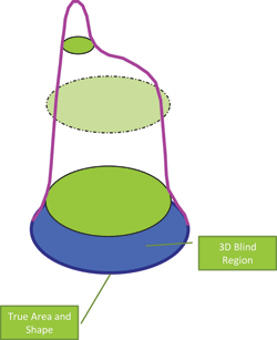
Perhaps the most critical advantage provided by the inclusion of 2D imaging is the dramatic improvement in zero referencing for the 3D measurements. 3D-only systems, because of their inability to analyse PCB surface layers and the difficulty in measurements of low heights, cannot determine the best zero levelling measurement location around each pad.
Height variations around a pad can be large, not only because of the variations caused by design (vias, solder mask, silkscreen legends and the pads themselves) but also variations caused by differences in individual PCBs and production batches.
3D-only systems estimate the zero reference level by averaging the height of a line surrounding the pad measured by golden board scanning. In 5D systems, by using 2D information, three or more reference points with equal base for height measurement can be used to set the zero reference, making them independent of varying heights between golden and production boards.

SPC for SPI
SPI has been proven of value in recent years not only to find print defects and improve end-of-line yields, but also as a process control tool that can reduce the occurrence of defects and thus improve overall print quality.

However, to be effective as a process control tool, the SPI system needs built-in real-time statistical process control (SPC) software that is easy to use. Typical generic offline SPC packages generally prove too difficult and too slow in use to be effective.
For example, by displaying a history of the previous 10 cycles as histograms, a quick understanding of the process stability can be gained. Cyclical and wide distribution of measured results can easily be spotted and understood.
CPK plots can provide understanding if a series of prints are stable and whether particular printing machine adjustments can provide more stable results. By changing one print setting at a time and running several boards after each change, the system enables the process engineer to readily gauge if the new setting provides increased or reduced stability.
A further improvement can be made if SPI and AOI data is merged to analyse if a defect found by AOI has its origin in the printing process or to readjust AOI tolerances upon inspection of certain solder joints.
5D SPI offers an improvement in ROI
With the introduction of 5D SPI, all categories of print process errors can be reliably identified and managed. Three dimensions (X, Y, Z) are needed to cover the wide range of printing defects and printing process errors.
Two dimensions (X and Y) are needed to cover errors linked to area, offset, smearing and bridging, while the third dimension (Z) is required to identify errors related to height and volume. Combining the best techniques to identify errors in each axis clearly improves the ROI for SPI equipment, and enables a new generation of closed loop process control.
The Marantz PowerSpector S1 employs the new 5D technology to deliver true area, shape, offset, volume and height measurement in one cycle.
This high-speed post-print solder paste inspection system incorporates patented new sensor technology and simultaneously combines 3D and 2D image processing methodologies for enhanced defect detection and process control.
Intercepting these defects before they happen reduces rework costs, provides yield improvement and accelerates return on investment.
The enhanced process control empowered by 5D technology provides a highly agile solder paste printer adjustment tool, enabling the correction of printer settings or paste problems before a problem spreads across an entire product.
| Tel: | +27 11 609 1244 |
| Email: | [email protected] |
| www: | www.zetech.co.za |
| Articles: | More information and articles about ZETECH ONE |


© Technews Publishing (Pty) Ltd | All Rights Reserved
 printer friendly version