


Digital signal processing (DSP) applications have always placed great demands on available technology. Ever-increasing system requirements drive an extraordinary degree of design optimisation to process data in real-time, and resulting systems usually employ a number of different processing technologies, each best suited to a particular function in the processing chain.
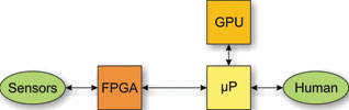
One of the most common forms of DSP application involves the gathering of information from sensors at very high data rates, processing this information into a form that is meaningful to humans and presenting this to the human at a much lower data rate. The traditional architecture for such a system is shown in Figure 1.

A field-programmable gate array (FPGA) is used for front-end ‘bit-rate’ or ‘chip-rate’ processing where data rates are highest and often presented as a continuous stream. FPGAs are programmed using a hardware description language (HDL) such as VHDL or Verilog, which allows state machines to be built up from combinations of logic blocks.
Programming in HDL is the hardware equivalent of programming in assembly language – the results are highly efficient (especially for low-level computations like FFTs and filters) but development requires great effort and HDL programmers are relatively scarce.
A DSP is used for front-end ‘symbol rate’ processing. DSPs are typically programmed using C or assembly language, but exploiting the efficiencies of these devices also requires careful programming considerations, often writing code specific to the device architecture.
A microprocessor is used for back-end ‘data rate’ processing and control. These allow the use of operating systems and high-level languages to provide a human-machine interface and access to data storage.
So, with reference to Figure 1, FPGAs show best efficiency (therefore smallest size and lowest weight), lowest power consumption and best determinism (lowest latencies).
However, because development time and cost are usually significant drivers in system design choices, much functionality is pushed in the direction of DSPs and CPUs, resulting in higher power consumption, more physical space, more weight, longer latencies and more execution jitter (indeterminism).
In deciding how to map functions to hardware, it should be noted that FGPAs work best when:
1. The computation is independent of the data, ie, there is little conditional processing and the algorithm can be expressed as a state machine.
2. The algorithm is mature. Developing and modifying algorithms using logic gates requires a considerable amount of effort compared to developing and modifying the same using a programming language.
This implies, conversely, that if an algorithm is data-dependent or subject to change then it is likely to be better implemented elsewhere than on an FPGA.
However, implementing a solution using three vastly diverse technologies requires development teams comprising three different specialised skill sets.
The resulting system also suffers from additional latencies introduced by interfaces between the three subsystems.
As the DSP component offers a compromise between the strengths of the FPGA and the microprocessor, it makes sense to investigate the possibility of removing it and implementing its functions elsewhere.
Where else can DSP functions be implemented?
A technology that has emerged from development in high-performance graphics processing is the graphics processing unit (GPU) and its less specialised cousin, the general purpose GPU (GPGPU). These devices can excel in processing large data sets where there is little interdependency in the data, but this restricts their use to a few specific applications.
They have very high power consumption and poor determinism because data is routed in and out of a microprocessor (see Figure 2). Efficiency is generally very poor, in practise only achieving less than 25% of theoretical performance for most applications.
A more common solution is to put microprocessor cores inside the FPGA as indicated in Figure 3. So-called ‘soft’ cores (programmed onto standard FPGA logic cells) are not an optimal use of available gates and generally enforce non-standard C-language implementations.

‘Hard’ cores (such as ARM devices implemented within the FPGA chip) might be useful for implementing protocol stacks but are not optimised for DSP functions as they have smaller feature sets and lower clock speeds than dedicated DSP chips.
High-level synthesis (HLS) tools, C-to-RTL tools and C-to-gates tools allow the implementation of algorithms in C language, but the C language is non-standard and the implementation usually involves a runtime module that is effectively a ‘soft’ CPU core being instantiated in the FPGA.
Neither of these solutions is particularly ideal.
The FPGA co-processor
A new approach is introduced here, as shown in Figure 4. In essence, an external multicore co-processor is coupled to the FPGA.
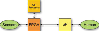
The co-processor allows the use of the C language to implement data-dependent algorithms while presenting itself to the HDL tools as if it were an embedded core. So, in some ways it resembles the embedded core approach discussed earlier, but an important difference is that it is optimised to provide highly efficient parallel processing capability.
Incorporating floating-point capability (DSP-friendly multiple/accumulate instructions) in the co-processor simplifies algorithm development. If the internal architecture of the co-processor allows the use of a standard C implementation while still achieving optimal performance, then the same developers can be used to code for both the microprocessor and FPGA co-processor.
It is important for the co-processor to allow fine-grained interaction with the FPGA by integrating directly to FPGA fabric, as many applications require data to flow back and forth between DSP and FPGA functions.
A multicore architecture is well suited to the inherently parallel nature of DSP algorithms and also provides for scalability. To make a multicore topology effective, a high-throughput mesh network is required so that data is available to all cores and synchronisation between cores is catered for.
Shared memory mapping should be transparent to the cores to simplify programming and memory should be cache-less to ensure determinism.
Another benefit of this approach is that immature algorithms ultimately destined for the FPGA can be implemented and refined quickly in code running on the co-processor. When the algorithm is stable it can then be ‘ported’ to an HDL implementation with little development risk.
An example in practice
The FPGA co-processor concept as described above has already been implemented and with very encouraging results. An example is BittWare’s Anemone AN104 chip based on the Epiphany architecture from Adapteva, which provides a 4 x 4 array of cores in a single chip.
Each core offers similar real-world performance to a TigerSHARC DSP. The AN104’s internal architecture is shown in Figure 5.

Board-level implementations are available from BittWare, which currently provides four Anemone chips on a single FMC module for a total of 64 cores to augment its existing Altera-based FPGA products.
Programming the Anemone does not require the use of any C subset, language extensions, SIMD or other ‘funny stuff.’ Standard GNU development tools are supported, including an optimised C compiler, simulator, GDB debugger with support for multicore, and an Eclipse multicore IDE.
Benchmarks for 8x8 matrix multiplication, 16-tap FIR filter, bi-quad IRR filter and 256-point dot product algorithms show between two and 10 times the code efficiency over SIMD architectures. It should also be noted that the implementation of the benchmarks required only one or two days’ effort each.
The Anemone AN104 shows enormous promise for this architecture, delivering a performance to power ratio of 24 to 32 GFLOPS/Watt compared to the best GPGPU solutions currently available around 20 GFLOPS/Watt (both figures here for single-precision floating point).
The next generation of the chip will implement 64 cores for an impressive 96 GFLOPS of double precision floating-point processing while achieving efficiencies exceeding 50 GFLOPS/Watt.
From what has already been demonstrated, the co-processor reduces system development costs and directly bridges the FPGA’s gaps of requiring algorithmic maturity and data independence by enabling out-of-the-box execution of applications written in regular ANSI C.
In other words: high efficiency, low power consumption and low latency with less development effort.
For more information contact Alastair Knight, Redlinx, +27 (0)21 526 4160, [email protected], www.redlinx.co.za


© Technews Publishing (Pty) Ltd | All Rights Reserved
 printer friendly version