
There are a number of circuits that require coupling RF signals or bypassing them to ground while blocking DC over extraordinarily large RF bandwidths. The applications for which they are intended typically require small, surface-mountable (SMT) units with low insertion losses, reflections and impedances across RF frequencies extending from the tens of kHz to the tens of GHz and temperatures typically ranging from -55°C to +85°C.
This article focuses on a particular implementation of these devices – multilayer ceramic capacitors (MLCCs) – and how to obtain the best performance when they’re used on various substrates.
Broadband capacitors are used in the ‘signal integrity’ market: optoelectronics/high-speed data; ROSA/TOSA (transmit/receive optical subassemblies); SONET (synchronous optical networks); broadband test equipment – as well as in broadband microwave and millimetre-wave amplifiers (MMICs, GaN transistors) and oscillators. The basic requirement in the former is to produce an output waveform that closely replicates an input waveform, typically a train of digital pulses, as shown in Figure 1.

While RF and microwave devices are typically measured in the frequency domain, digital systems are usually characterised in the time domain and so it is necessary to make a connection between the two (Figure 2).
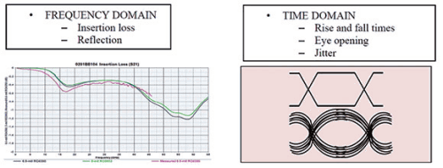
Fortunately, all electrical engineers are familiar with the Fourier and Laplace transforms that do precisely that. The low-frequency and high-frequency responses required to reproduce a train of rectangular pulses with reasonable fidelity are shown in Figure 3.

In general, systems that transmit all frequencies with equal velocity and minimal attenuation and reflection will accurately reproduce input signal waveforms at their outputs. Conversely, systems that are dispersive, i.e., where signals at different frequencies travel at different speeds or have unequal attenuations or reflections, create distortions in the output waveform.
Broadband capacitors
In considering ‘broadband capacitors’, perhaps the first question that arises is precisely what distinguishes these devices from any other capacitors. One property is alluded to above: when used to RF couple/DC block, the capacitor should have minimal attenuation and reflection. Figure 4 compares the insertion loss vs. frequency plot of a typical high-Q ceramic microwave capacitor with that of a broadband capacitor.
The salient feature of the plots is that the high-Q capacitor exhibits a number of ‘parallel resonances’ that create regions of high insertion loss, which is not the case with the broadband device.

A lumped-element electrical model
To understand the electrical behaviour of an MLCC, one place to begin is with an equivalent circuit that produces the same performance, including interaction with a microstrip or coplanar waveguide transmission line. One such circuit, using lumped elements, is shown in Figure 5.

If we consider a reduction of this circuit to only the first (lowest order) branch, Cg can be considered to represent capacitance of the MLCC body to the groundplane; C, the capacitor’s value; L, its net inductance in the presence of the groundplane; and R, the equivalent series resistance (ESR). Note that to more closely reflect actual performance, L and R are both frequency varying to accommodate skin and proximity effects.
The addition of a second branch consisting of another inductor, Lp1, in series with another capacitor, Cp1 and resistor Rp1, enables modelling the lowest-frequency parallel resonance; addition of additional Lpn-Cpn-Rpn branches capture higher-order parallel resonances.
There are, however, constraints on these higher-order element values beyond yielding the correct resonant frequencies, e.g. the model’s low-frequency capacitance value (all inductive reactances negligible) must equal the true low-frequency value of the device and the high-frequency inductance value (all capacitive reactances negligible) must also equal that of the device.
Both broadband and high-Q MLCCs have the same physical structure: interleaved metallic electrodes embedded in a ceramic brick. From whence, then, comes the difference in behaviour? Examination of Figures 4 and 5 suggests at least one answer: the broadband capacitor is lossy.
Specifically, in Figure 5, resistances Rp1 through Rpn must be high enough that only exceedingly low-Q parallel resonances are created when their reactances are capacitive and those of the lower branches are inductive. If this is the case, then at frequencies high enough that the reactance of C is negligible compared to that of L, the circuit reduces to the simple one in Figure 6.
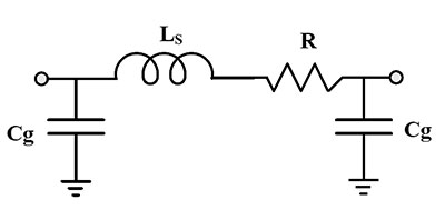
It may be observed that this is a lumped element (low-pass filter) approximation of a transmission line section and, as such, best performance should be achieved by having the characteristic impedance of that section, (Ls/Cg)1/2, about equal to 50 Ω.
While lumped-element models are quite flexible, particularly where element values can incorporate arbitrary variation with frequency, there is at least one reason to be wary in applying them to broadband capacitors: the models are ad hoc, heuristic representations, derived from a combination of experimental observations and ‘common sense’ circuit theory (there must be some series inductance, there must be some shunt capacitance to ground, etc.), rather than more fundamental principles. Nowhere is this clearer than in the addition of the Lp-Cp branches to create parallel resonances. As lumped elements, they have no obvious physical origin and are attached ad hoc purely to simulate observed electrical manifestations.
We should, in fact, be cautious about any lumped-element representation of capacitors that operate at sufficiently high frequencies – but let’s consider where ‘sufficiently high’ might begin. Typical X7R dielectrics for these devices have relative dielectric constants in the 2500-3000 range. This implies quarter wavelengths on the order of 60 mils or less at 1 GHz. Thus, an 0402 device of length 40 mils would reach a quarter wavelength at 1,5 GHz; a 20-mil-long 0201 device would reach a quarter wavelength at 3 GHz. It therefore seems evident that, to characterise these devices to 50 GHz and beyond, we’d really like a distributed model.

Distributed electrical models
Figure 7 depicts how an idealised, lossy, open-circuit series stub can function as a broadband coupling device. Note the resolution of the apparent paradox: how can the stub itself be quite lossy and yet have only minimal effect on the main line? The answer is that as long as the stub characteristic impedance is low relative to the main line characteristic impedance, the main line insertion loss will also be low. In fact, if the stub loss is sufficiently gradual and large, the stub input impedance will approach its characteristic impedance.
Turning now to distributed capacitor models, one such was proposed many years ago by Gordon Kent and Mark Engels.[1],[2] Using a procedure involving ‘unfolding’ the interleaved electrode structure of the capacitor, they arrived at an equivalent section of open-circuited parallel-plate transmission line that exhibited periodic series and parallel resonances.
This model had, however, a number of drawbacks: (1) It considered a capacitor only in isolation, not including interaction with the substrate it was mounted on; (2) it did not account for the fact that observed parallel resonances do not occur at uniformly spaced frequencies (again, ad hoc reactances or line sections were added in an attempt to model the latter behaviour); and (3) it required the currents in each electrode to flow in opposite directions on each surface, something impossible at frequencies below those where significant skin effect occurs – and yet where parallel resonances are nevertheless observed.
Alternative distributed models consider the Lpn-Cpn-Rpn branch circuits of Figure 5 as the capacitances, inductances and resistances of individual overlapping electrode pairs, all loading an open-circuited parallel-plate stub transmission line formed by the MLCC terminations.
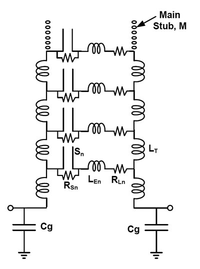
Figure 8 is an example of one such model. In this case, the interleaved electrodes also have quasi-distributed representations (open circuit stubs instead of lumped capacitors) in accordance with models of metal-insulator-metal (MIM) capacitors.[3]
Referring back to our discussion of open-circuited series stubs, it may be observed that if the characteristic stub impedance Z0M is << 50 Ohms, the internal distributed losses can be large and yet the overall insertion loss as a series-connected device will be low. (The impedance at the input to stub M will simply approach a Z0M Ω resistor.) Therefore, another part of making a capacitor broadband is reducing LT and LEn as much as possible, while maintaining high capacitance.
Unfortunately, neither lumped nor distributed theoretical models are able to capture the full range of real-world complexity: the presence of three different dielectrics (capacitor, air, substrate) and consequent TEM propagation modes;[4],[5] the mutual inductance and resistance effects of the electrodes; the discontinuity reactances of the microstrip-to-MLCC transitions (including solder joints); mounting pad dimensions that exceed those of the device’s termination footprints; higher (non-TEM) mode generation; radiation; etc.
However, there is a combined experimental/theoretical approach, e.g.,[6] that does yield good agreement with real-world behaviour: it is that taken by Modelithics, a vendor that creates electrical models based on extensive (soldered on) device measurements performed on a variety of substrates having different dielectric constants, thicknesses and pad dimensions.
PPI has commissioned Modelithics to measure and model a number of its broadband capacitors; in the following section, by investigating the behaviour of one such model under several different conditions, we can arrive at some fundamental conclusions on how to achieve good performance.
Optimising performance as a coupling/blocking device
We will use the Modelithics model of the PPI 0201BB104 broadband MLCC to derive some general principles as to how best to achieve our objective. Two circumstances must be addressed: (1) The user has the freedom to select a substrate best suited for a broadband capacitor; or (2) the user already has a substrate and wants to optimise performance with a broadband capacitor. In each case, the user must know the highest operating frequency; this will determine the required characteristics of both substrate and broadband capacitor.
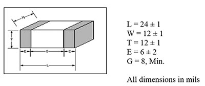
To achieve our objective, we modelled performance – insertion loss and return loss – of the PPI 0201BB104 on microstrip substrates having three different dielectric constants. Three thicknesses of each substrate were chosen to create the following conditions with respect to the trace width necessary for a 50 Ω characteristic impedance transmission line (at 10 GHz): equal to the part width, less than the part width, greater than the part width. Figure 9 shows the basic dimensions of the part; while Table 1 provides specifics on the substrates.


It is seen that, in all cases, best performance (red curves) is achieved when the part width is about the same as W50, the 50 Ω characteristic impedance trace width. If the part width is either significantly greater than W50 (blue curves) or less than W50 (green curves), performance is degraded. Note that this is roughly consistent with the very simple circuit of Figure 6 and the seemingly naïve observation above it that best performance would be obtained when (Ls/Cg)1/2 was about equal to 50 Ω. (The caveats, however, still apply: the Figure 6 circuit does not predict details of the frequency response.)
Mounting pads and impedance matching
In light of the above, there is no one-size-fits-all prescription for mounting pad dimensions because there are too many variables involved: PC board dielectric constant and thickness, customer pick-and-place capabilities, PC trace tolerances, performance desired over frequency range, etc.
In general, for good (but not necessarily optimum) performance, one wants the width of the part and mounting pad to be about equal to the width of a 50 Ω trace on the substrate and the lengths of the lands to extend only minimally beyond the length of the part. As for the gap, 5-mils nominal is a good starting point for the 0201BB104 and 01005BB104 – although (again) not necessarily the absolute optimum – while a 10-mil gap is a good starting point for the 0402BB103 and 0402BB I 04.
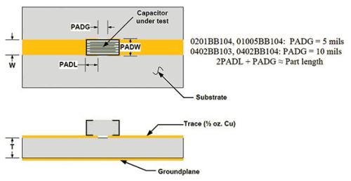
Figure 13 illustrates these suggestions.
It may be of interest that the 020 lBB 104 Modelithics model has a pad scalability feature, meaning that the landing pad dimensions can be changed within prescribed limits and the consequent electrical behaviour characterised. Note that the minimum and maximum dimensions on the Modelitliics pads – PADL, PADW, PADG – are simply the ranges over which the model is valid, not recommended tolerances. Keep in mind, too, that the part itself has the tolerances shown in Figure 9.
Determining final pad tolerances often devolves to a struggle between RF engineers, who want the pad width and tolerance to match as closely as possible the part width and tolerance and production processing engineers, who’d like the largest pad dimensions and tolerances possible to facilitate pick-and-place operation.
Fortunately, performance over most frequency ranges through about 40 GHz seems relatively insensitive to small deviations of pad dimensions. If the substrate thickness and trace width are determined before the broadband capacitor is selected, then it’s best to choose a capacitor whose width is closest to that of the 50 Ω trace.
There is also the possibility of improvement if additional impedance matching is done. In general, when the part width exceeds the trace width, the imaginary part of the input impedance is capacitive and the creation of additional series inductance by a short section of reduced trace width can help.
Alternatively, removal of a portion of the dielectric beneath the capacitor (reducing the shunt capacitance to ground) can also be effective. Similarly, when the part width is less than the 50 Ω trace width, the input impedance is inductive and the creation of additional shunt capacitance by widening a section of trace width adjacent to one or both mounting pads, or the mounting pad widths (PADW) themselves, can improve performance.
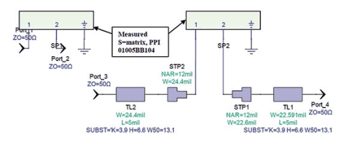
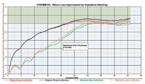
An example of impedance matching is shown in Figure 14, which applies to PPI model 0l005BB104, a 100 nF EIA size 01005 part mounted on a 6,6 mil thick substrate of dielectric constant 3,9. The part itself is 8 mils wide and the trace it was mounted on was 12 mils wide. (The 50 Ω trace width on the substrate at 10 GHz is 13,1 mils.)
Using a scattering matrix for the part measured by Modelithics, return loss was plotted in Agilent Genesys software for (a) the part alone, and (b) a circuit that adds 5-mil-long sections of widened traces at input and output. Using Genesys ‘s optimisation function, dimensions of the traces were adjusted for best input and output return loss over the 0,05 to 46 GHz measurement range.
It should be cautioned that, because of the part’s insertion loss, input reflection after impedance matching at only one port is not necessarily equal to output reflection; one could improve return loss at one of the ports beyond that shown, but the improvement would come at the expense of the other port’s reflection.

Non-linear behaviour - VCC, temperature, ageing
Thus far, we’ve discussed only the basic electrical performance of broadband capacitors as linear devices but, particularly where so-called ‘signal integrity’ is important, e.g. in accurately reproducing a stream of (rectangular waveform) bits from input to output, a number of non-linear parameters are involved. Let’s define the major ones before proceeding to some of the trade-offs involved:
• The voltage coefficient of capacitance, VCC, is the change of capacitance – usually a decrease – with applied voltage. In general, VCC depends on the electric field (volts/mil) across the dielectric and the higher the dielectric constant, the greater the VCC. Any decrease in capacitance is likely to impact the low-frequency range of performance. Figure 15 shows the capacitance change with DC voltage for three PPI broadband MLCCs. Capacitance will also change with AC voltage and frequency, sometimes rising with the latter before falling off.
• The temperature coefficient of capacitance, TCC, is the change of capacitance with temperature. In general, the higher the dielectric constant, the greater will be its change with temperature. Most broadband capacitors have dielectrics rated as either X7R, signifying a ±15% maximum capacitance change with temperature from -55°C to +125°C, or X5R, signifying a ±15% maximum capacitance change with temperature from -55°C to +85°C. Again, any decrease in capacitance will impact the low-frequency range of performance.
• Ageing is the tendency of non-linear dielectrics, e.g. the X7R type, to exhibit a reduction in dielectric constant as time passes. It is usually given in ‘percent capacitance loss per decade hour,’ implying that, on logarithmic graph paper where time is the ‘X’ variable and capacitance is the ‘Y’ variable, there is a straight line characteristic with a negative slope.
Ageing is typically measured starting from 10 to 24 hours after a capacitor emerges from an oven set at a temperature above that of the dielectric’s Curie temperature. Thus, a capacitor will lose capacitance by the same percentage from 10 hours to 100 hours as it will from 100 to 1000 or 1000 to 10 000.
In order to be sure that customers receive a stable part, most manufacturers wait till the fourth decade, so that the part’s age is between 1000 and 10 000 hours before shipping. Nevertheless, when thinking about performance over shelf time at the factory and subsequent field life, customers should be cognisant that over 10 000 hours – about 14 months – capacitance values may, in the worst case (original shipment after 1000 hours), decrease by the ageing specified maximum percentage.

Table 2 indicates some of the trade-offs in design and selection of a broadband capacitor. The left-hand column contains independent parameters; the boxes show the results if any one parameter is changed as shown while the others are held constant.
In general, larger capacitance values enable operation down to lower frequencies. To extend the upper operating frequency, smaller case sizes are needed, since these are commensurate with the smaller substrate thicknesses and narrower line widths required for higher-mode-free, high-frequency operation. Therefore, to extend both ends of the spectrum, one must squeeze equal or greater capacitance into smaller case sizes and the only ways to accomplish this are to either decrease the inter-electrode dielectric spacing and/or use a dielectric with a higher dielectric constant. The first reduces the voltage rating (WVDC) and either approach exacerbates the non-linear effects – and thus the trade-offs.

Performance as a bypass device
It is often desired to bypass some point to ground over a large frequency range, that is, provide a path having very low impedance to RF signals while still blocking DC. In the past, this was typically accomplished by an array of capacitors having different values, as shown in Figure 16.
Here, Cl might be perhaps 100 pF, C2 might be 1 nF and C3 might be 10 nF. There were two problems with this arrangement: (1) Above the series resonance of C3 [= (2π)-1(L3C3)-0,5], its impedance was inductive and would create a parallel resonance with Cl and C2; and (2) the individual capacitors had their own built-in parallel resonances.
Either problem led to an impedance magnitude vs. frequency characteristic similar to that shown on the right of Figure 16. To reduce the magnitude of the resonances, additional loss would need to be introduced in the form of low-value resistors connecting the capacitors or ferrite beads surrounding the connecting leads. In contrast, broadband capacitors offer a simple, cost-effective way to replace these arrays with a single capacitor.
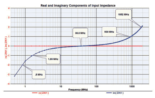
Again using the Modelithics model of the PPI 02018B104 on a 6,6 mil thick, K=3,9 substrate, this time with a grounded output, Figure 17 shows the real and reactive parts of the input impedance.
It is seen that the reactance is inductive above 38,6 MHz and capacitive below that frequency; it is the magnitudes of these
components that will determine the operational range. For example, if the absolute value of the impedance to ground needs to be <1 Ω, the frequency range over which this is achieved is 1,86-930 MHz; if the value can be extended to <2 Ω, the frequency range can be commensurately widened to cover 0,8-1852 MHz. Note that the plots do not include the inductive contribution of a via to the groundplane, which is likely required in many practical situations.
The inductive reactance could be reduced by decreasing spacing to the groundplane (although 6,6 mils is already quite thin) and total reactance can be reduced by paralleling two or more devices, but the latter may not be practical for reasons of space or economics. In summary, in a bypass mode, a broadband capacitor can effectively replace an array of capacitors to cover frequencies ranging from the high kHz/low MHz region to the low GHz region, depending on the requirements of the particular circuit.
Conclusions
The principal ‘take aways’ from the discussion are listed below:
• Used as DC blocking/RF coupling devices, SMT broadband ceramic capacitors can operate free of parallel resonances over a very wide frequency range. Resonances are suppressed by losses within the device.
• Circuit models, whether lumped or distributed, cannot adequately capture the effect of all the electrical phenomena involved in practical devices: mutual inductance and resistance of the electrodes; discontinuity reactances of microstrip-to-MLCC transitions (including solder joints); mounting pad dimensions that exceed those of the device’s termination footprints; higher (non-TEM) mode generation; radiation; etc.
• Good experimental/theoretical combination models, such as those available from Modelithics, enable performance simulation on a variety of substrate thicknesses and dielectric constants. Impedance matching can often be used to improve insertion loss and return loss performance.
• Non-linear effects – capacitance change with applied voltage, temperature and time passage – can negatively affect performance. Trade-offs can be made that impact maximum working voltage and case size.
• In a bypass mode, a single SMT ceramic capacitor can replace an array of various-value capacitors to effectively cover frequencies ranging from the high kHz/low MHz region to the low GHz region.
References
[l] M. Ingalls and G. Kent, ‘Monolithic Capacitors as Transmission Lines,’ IEEE Trans. Microwave Theory Tech., vol. MTT-35, pp. 964-970, Nov. 1987.
[2] M. Ingalls and G. Kent, ‘Measurement of the Characteristics of High-Q Ceramic Capacitors,’ IEEE Trans. Components, Hybrids, and Manufacturing Technology, vol. CHMT-12, pp. 487-495, Dec. 1987.
[3] A. Murphy and F. Young, ‘High Frequency Performance of Multilayer Capacitors,’ IEEE Trans. Microwave Theory Tech., vol. MTT-43, pp. 2007-2015, Sept. 1995.
[4] V.K. Tripathi, ‘Assymetric coupled Transmission Lines in an Inhomogeneous Medium,’ IEEE Trans. Microwave Theory Tech., pp. 734-739, Sept., 1975.
[5] V.K. Tripathi, ‘Equivalent Circuits and Characteristics of Inhomogeneous Nonsymmetrical Coupled-Line Two-Port Circuits,’ IEEE Trans. Microwave Theory Tech., pp, 140-142, Feb., 1977.
[6] B. Lakshminarayanan, et al, ‘A Substrate-Dependent CAD Model for Ceramic Multilayer Capacitors,’ IEEE Trans. Microwave Theory Tech., vol. MTT-48, pp. 1687-1693, October, 2000.
| Email: | [email protected] |
| www: | www.trxe.com |
| Articles: | More information and articles about TRX Electronics |

© Technews Publishing (Pty) Ltd | All Rights Reserved