
Today’s bandwidth boom – 400G rollouts, 5G and the explosion in data centre development – is being driven in large part by photonic integrated circuits (PICs). Tiny but mighty, these powerful components are fuelling our telecom future.
This disruptive technology has been picking up pace in recent years, primarily in telecom applications, but also in the medical, sensing and military sectors. Often compared to the ground-breaking electronic processor, PICs are similarly created on wafers before being cut into individual chips.
PICs bring photonics into the realm of integrated electronics by merging, in a compact design, photonic components such as lasers and modulators with opto-electronic, electro-optical, fully electronic or even RF functionalities and endless potential in applications ranging from medicine to data centres, autonomous cars and quantum computing.
Testing such a maelstrom of complex components poses many challenges, however. Testing key parameters on the myriad of active and passive optical, electronic or RF components contained on each chip can be tricky.
In the early days of PIC development, design, manufacturing and testing were performed by academic or highly specialised research groups. Through a lengthy and cumbersome process, test and measurement engineers working with PICs often needed to create their own custom solutions. With today’s growing pressure to churn out the technology, the test and measurement of PICs needs to happen much faster and become more reliable.
When it comes to optical characterisation of PICs, several test solutions and measurement methods exist. This article covers the basic principles of optical testing directly on wafers and the best measurement methods for both active and passive components present on the PIC chip.
PIC basics
A PIC is a compact photonic system that enables complex functionalities by combining tens, hundreds or even thousands of individual components onto a single thumb-sized chip. Much like electronic integrated circuits (EICs), PICs are manufactured on wafers that can contain several hundreds of chips. However, unlike their electronic counterparts, the key advantage of PICs is the ability to combine their optical functionalities with electronic and RF features in a compact design.
Active optical components (i.e., light emitting) such as lasers or amplifiers are typically manufactured on indium phosphide (InP), whereas silicon photonics (SiPh) are the weapons of choice for all passive optical structures such as modulators or ring resonators. The choice of substrate material also strongly depends on the final application and wavelength of operation (visible, near infrared or infrared).
Apart from the obvious compactness of the chip compared to equivalent bulk optical components, PICs also offer advantages including low cost and operating power and mass volume production with high reproducibility. They also allow for the design of particular optical structures that are not achievable with conventional optics.

PIC technology is developing fast. Figure 1 illustrates the types of building blocks already available. Combining these components on the chip creates the required features and functionalities for:
• Simple waveguides, delay lines, splitters and multimode interference couplers.
• Mux/demux, usually based on arrayed waveguide gratings (AWG).
• Electro-optic modulators based on either a Mach-Zehnder interferometer or ring resonators.
• Photodetectors that can be inscribed onto the chip for in-chip optical power monitoring.
However, there are still a few hurdles to unlocking the full potential of PICs. Photonics have some stringent limitations due to light itself: it is not as easy to manipulate photons as it is to play with electrons. Coupling light in and out of a device using optical fibre with a 10 µm core requires expertise.
This makes the whole business of testing and packaging PICs more daunting and test and measurement of those chips has become a bottleneck in the whole PIC development. Even more so because those characterisations need to be addressed in a way that would allow hundreds of thousands of components to be made every year.
Those types of building blocks have been used in the telecom industry for more than a decade to create complex systems such as transceivers and tuneable lasers. PICs lend themselves particularly well to the field of telecommunications because they can cope with the challenges the industry faces: the ever-increasing need for compact devices, higher bandwidth and energy efficiency for high-speed networks. 5G and the increase in data rates from 400G to 800G and beyond in data centres and the rest of the network depend on efficient PIC development from design to packaging.
Applications
As a maturing technology, PICs now offer a great deal of potential in sectors outside of telecoms, including sensing, government and military applications, medical and bio imaging and lidar, which is becoming more prominent with the advent of autonomous cars.
The explosion of potential applications has inspired government initiatives, mostly in the US and Europe, to support the growth of companies and businesses working with all aspects of PICs – from design and R&D; to high-volume manufacturing. As a result, PIC technology is moving ever quicker from the university lab to the mainstream.
PICs: testing and challenges
The bandwidth boom and push to grow this technology has put stricter demands on test and measurement of these devices. Manufacturers and operators now need to have faster, more reliable methods for testing than ever before.
Testing: a crucial step in any PIC project
TAP (test, assembly and packaging) constitutes up to 80% of the total cost of device production. Testing is an integral part of each phase of a PIC project, from design and fabrication in PIC foundries to assembly and packaging. Foundry engineers perform tests directly on the wafer to improve fabrication processes and establish tolerances and limits to the properties of each device. Those test results are fed back into process design kits (PDKs), which are essentially databases of optical-electronic characteristics for optical components that allow accurate modelling of the final chip properties. Functional testing is performed at the packaging stage to check devices before they are shipped to the customer.
This testing is similar to typical passive component testing for specs and reliability (fibre in/out or electronic in/out testing).
Wafer-level testing
Testing at wafer level is the most cost effective and efficient. Even if it requires specialist equipment to perform key parameter measurements, hundreds of PICs can be characterised and selected automatically. It is even possible to perform more advanced testing directly on the chip on the wafer to truly validate the die.
Testing devices across a wafer, from edge to centre, provides key information about the chip fabrication process. When testing a wafer produced for research purposes during development, a lot of information can be gathered about what process issues occurred or what anomalies were introduced by using a particular production recipe. This helps to link acceptable processes and tolerances to defects or anomalies.
The goal of wafer-level testing during production is to separate bad chips from good ones so that defective PICs can be discarded as early as possible, as dicing and packaging a bad device can prove very costly. Testing PICs on an industrial scale needs to be quick and reliable. With so many chips to test, separating good chips from bad ones is critical.
Probe stations have been developed extensively for electronic applications, such as CMOS (complementary metal-oxide-semiconductor) wafer testing, but upgrading those systems to perform photonic coupling in and out of the device is a whole new challenge.
First, the precision of the alignment system is critical as the size of the photonic coupling points are much smaller than electronic test pads. Second, the optical coupling is performed using optical fibres with cores of 10 µm in size that require 6-axis alignment (see the ‘Did you know?’ sidebar).
Did you know?
How light is coupled in and out of devices on the wafer
Optical fibres are used to transport light from the source to the wafer and from the wafer to the optical component tester. These fibres, with 10 µm cores, need to line up with a test point on the wafer. An efficient test point consists of an optical grating coupler inscribed onto the wafer surface.
The optical fibre is aligned on top of that test point at an incidence of 8 degrees to ensure best light coupling efficiency, typically 1,3 dB of optical loss. The same method is used to couple light out of the device. When testing a complex device with many inputs and outputs, an array, or bundle, of optical fibres can also be used in place of a single fibre to couple into several of these grating couplers simultaneously, which allows for testing of multiple functionalities and ins and outs at the same time.
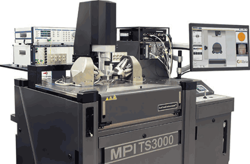
Once the alignment part of the test is complete, optical characterisation can begin. This is shown in Figure 2 with EXFO’s CTP10 component testing platform. Automation of the test process is then achieved by controlling all equipment from custom software on a PC.
Advantages of using photodiodes
Photodiodes can easily be inscribed onto the wafer and can be used to simplify and/or speed up the test process. These devices, positioned through the device’s optical path, constitute test points that aren’t necessary to couple out of the system into an optical fibre, saving precious test time: photodiodes in the optical path can replace grating couplers. They require no precise alignment on electrical pads and are more robust than a fibre. Furthermore, these are test points that can then be easily cut out on the finished PIC product. Several photodiodes on a chip can also be lined up to facilitate testing, in the same way that optical grating couplers can be lined up to a fibre array.
PIC key parameters: what to test
Parametric testing
The fundamental characteristic of an optical component is its spectrum as a function of wavelength. For active components such as lasers or amplifiers, the spectrum is a measurement of the optical power output as a function of wavelength.
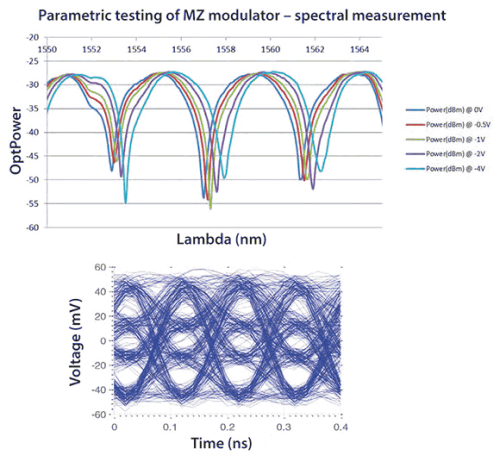
For passive components (components not generating light), the measured spectrum corresponds to the insertion loss (IL), which refers to the ratio, expressed in decibels (dB), of transmitted light to incident light resulting from the insertion of said device. It can also be of interest to measure the spectral footprint of the component’s return loss (ratio of light reflected by the device) and polarisation-dependent loss (variation of insertion loss due to polarisation of the light). Spectral analysis of passive components yields results such as optical finesse, peak wavelength, passband characteristics, on/off ratio, filter isolation, filter bandwidth, etc.
Functional testing
Wafer-level testing can also include functional testing from the start, if the design of the device allows it. For example, an MZ interferometer can be used as a modulator directly on the wafer and functionally tested by using a BERT and sampling scope to analyse the resulting eye diagram – this to further reduce the risk of integrating a defective chip.
Challenges and testing methods for PICs
Today, there are various solutions to perform state-of-the-art parametric or functional testing. As discussed, PIC manufacturers are looking for ever faster, ever more reliable ways to characterise those components. In the following, we will describe the parametric test techniques best suited to those new devices.
Manufacturers are looking for flexibility, reliability and speed. They also want to make sure all PICs are tested in the same simple way and that results can be trusted.
1. Testing active components of PICs
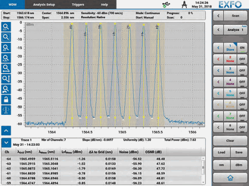
Testing active components such as lasers and amplifiers found on PICs is very simple and is done with an optical spectrum analyser (OSA). Spectrum analysis of these active devices yields specific device information. The transceiver internal laser is checked for centre wavelength and side mode suppression ratio (SMSR). Additionally, WDM signals, created using AWG structures, are checked for optical signal-to-noise ratio (OSNR).
An OSA can be used to perform tests on active components simply by connecting the light source or laser output to the OSA to get the spectral signal of the sources, as seen on the right of Figure 4. Leading OSAs have the advantage of being very fast, performing up to five scans per second at speeds of 2000 nm/s, fast enough for real-time component alignment and with a high enough resolution to allow measurement of key parameters such as OSNR and SMSR.
2. Testing passive components of PICs
OSA-based passive component characterisation
It is also possible to use an OSA for passive component testing. The OSA is used with a broadband source (i.e., with some power over a broad wavelength range) with a very large, flat spectrum and stable power. When coupled into the chip, the light can be collected and coupled to the OSA. The OSA will then perform a sweep to record the spectral response of the device under test (DUT).
This technique has the advantage of being very fast, but falls short when it comes to measurable dynamic range and spectral contrast, control over polarisation and the fact that only one output can be tested at a time, making it impractical for some PIC applications with a high port count.
Stepped laser method
One method already being used in standard, non-PIC, passive component testing is the stepped laser technique. The method circumvents the issues of the OSA technique: the laser can be used with a detection system composed of several hundred power meters if required.
All the power is concentrated into a single wavelength, meaning that the dynamic range is very wide due to laser optical power density. It provides good spectral coverage by combining several lasers to achieve measurements between 1250-1700 nm most of the time. Finally, it is also very easy to control polarisation since the laser is highly polarised and hence, perform PDL measurements. Stepped measurements rely on a tuneable laser that is successively tuned to various wavelengths.
The method provides excellent results for coarse spectral sampling (>100 pm), and when used in conjunction with external cavity lasers (ECL), can perform measurements in a few minutes over a broad spectral range and with good dynamic range. This technique however is too slow when the component under test calls for a higher resolution (typically, 1 pm [picometre] or even less). For ring resonators with a sharp, picometre-scale spectral response, this is a significant limitation.
Swept wavelength method
To take reliable measurements for today’s complex components, the most efficient and effective option is the swept laser technique, illustrated in Figure 5. This method uses a continuously tuneable laser source in conjunction with a component tester that records wavelength and power detection synchronously as the wavelength is scanned through with the laser. It can achieve picometre spectral resolution with a very large optical power dynamic range within seconds.
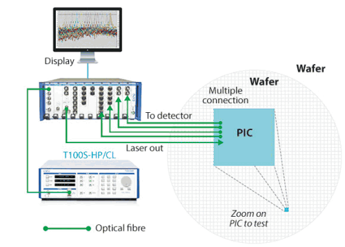
The advantages of using a continuous tuneable laser are combined with benefits for the component tester itself. This device is a specialised instrument with very short test times and excellent accuracy: it records the test wavelength and output power simultaneously as the laser is being swept, as opposed to a stepped wavelength measurement where the laser is moved one step at a time.
A larger spectral range, important when characterising components spanning all telecom bands, can also be tested using several tuneable lasers, each covering a portion of the total spectrum under test and concatenating the insertion loss or return loss result into a single spectrum. What’s more, it is the only method that provides picometre-resolution PDL spectra within a reasonable timescale.
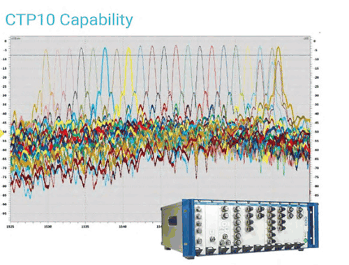
Figure 6 illustrates what can be done with a component tester. In this case, the customer wanted 25 channels tested simultaneously in a single scan. The CTP10 covered the full dynamic range with 1nbsp;picometre resolution in 2nbsp;seconds.
The future of PIC spectral testing
The endless potential of photonic integrated circuits means that the demand for these powerful components is huge and there is a big push to further develop the technology. Because PICs combine a range of photonic and electronic components, testing them is very challenging. Given the growing demand for PICs and their speedy evolution, having more reliable, faster testing solutions is now crucial.
It is clear from these developments that ‘designed-according-to-test’ PIC chips are key in reducing testing time while boosting reliability. Symbiosis between design, fabrication and testing is the path to understanding and addressing any issue throughout the PIC development process. The same holistic approach can be applied during PIC assembly and the final packaging of the component to further reduce the impact of TAP on the final chip cost.
© Technews Publishing (Pty) Ltd | All Rights Reserved