Four reasons for X-ray inspection of surface mount devices
25 February 2015Manufacturing / Production Technology, Hardware & Services
Vision inspection systems can find visible defects on PCBs, but these systems can only check the surface for errors, not the hidden solder joints of components like BGAs and flip chips. X-ray inspection can provide critical verification of the integrity of hidden solder joints on surface-mount devices.
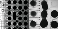
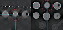
Figure 1. Solder ball shorts.
The following are four of the most common examples of faults that X-ray inspection is best suited to detecting.
1. Solder ball shorts
Solder ball shorts, or solder bridges, can be easily detected with an X-ray image, as shown in Figure 1.
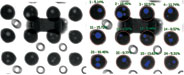
2. Solder ball voids
Figure 2. BGA void image with auto void calculation.
Ball-void inspection is used for BGA/CSP inspection along with solder ball bridge inspection.
Modern X-ray inspection systems can perform auto ball-void calculations (Figure 2).
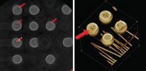
Figure 3. BGA void location.
Not only is the size of the BGA voiding area important, the location of the BGA void is also important (see Figure 3), especially if the voiding area is close to the PCB pad area, because there is a possibility that this voiding area could cause a micro-crack.
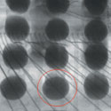
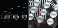
Figure 4. Solder ball open.
3. Solder ball open / micro cold solder
Solder ball attachment to the PCB pad is a critical inspection criterion. A high-resolution and high-magnification X-ray inspection system is required to detect a solder ball open defect. The X-ray image in Figure 4 shows a solder-ball open where the copper pad is separated below the solder ball.
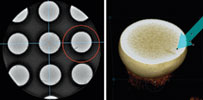
Figure 5. Solder ball open caused by small solder ball.
3D CT can assist with clear visualisation of open patterns. Figure 5 shows a solder ball open caused by the solder ball being too small. The image on the left shows a Y-Z slice image, indicating that the solder ball is smaller than the other ones. The image on the right shows an X-Y slice, indicating that the PCB pad (dark area) is not surrounded by a solder ball (white edges).
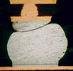
Figure 6. Cold solder – optical image.
Micro cold-solder joints can also be visualised with 3D CT, as illustrated in Figures 6 and 7.
Figure 7. Cold solder – non-destructive 3D CT image.
4. Solder ball crack
Using oblique CT technology, a solder ball crack can be visualised. Figure 8 shows a 10 micron solder ball crack.
Revolutionising clean air in electronics manufacturing Allan McKinnon & Associates
Manufacturing / Production Technology, Hardware & Services
Designed to prioritise clean air in the electronics manufacturing industry, the ZeroSmog Shield Pro sets a new standard for workplace health and safety.
Read more...High-speed multi-function dispensing Techmet
Manufacturing / Production Technology, Hardware & Services
The D-VIS and DL-VIS from GKG SMT printer specialists are high-speed dispensing systems that can handle multiple scenarios.
Read more...Optical inspection for SMT Techmet
Manufacturing / Production Technology, Hardware & Services
The Xpection 1860 from Scienscope is a versatile X-ray inspection machine that offers comprehensive circuit board defect detection and quality assurance for the SMT industry.
Read more...Yamaha introduces upgrades to its 3D AOI systems Truth Electronic Manufacturing
Manufacturing / Production Technology, Hardware & Services
Yamaha Robotics SMT section has revealed performance-boosting upgrades for the YRi-V 3D AOI system, including faster board handling, multi-component alignment checking, and enhanced LED coplanarity measurement.
Read more...Flexible printed electronics substrates
Manufacturing / Production Technology, Hardware & Services
New LEXAN CXT film from SABIC offers high thermal process stability and transparency for demanding printed electronics substrates.
Read more...Lead-free solder paste Techmet
Manufacturing / Production Technology, Hardware & Services
Indium8.9HF is an air reflow, no-clean solder paste specifically formulated to accommodate the higher processing temperatures required by SnAgCu, SnAg, and other alloys.
Read more...Analog Devices and Mouser collaborate on eBook
Manufacturing / Production Technology, Hardware & Services
Mouser has released a new eBook in collaboration with Analog Devices, that offers a detailed analysis of the technologies being used to support sustainable manufacturing practices.
Read more...Improved precision laser marking RS South Africa
Manufacturing / Production Technology, Hardware & Services
On-the-fly marking at high speeds is only one of the comprehensive features of Panasonic’s new LP-RH laser marker series.
Read more...Optimising AOI performance Rugged Interconnect Technologies
Manufacturing / Production Technology, Hardware & Services
Optimising AOI performance is now a reality with the highly integrated ADLINK MVP-6200, combined with Intel Arc GPUs.
Read more...High-mix SMT solution from Panasonic Techmet
Manufacturing / Production Technology, Hardware & Services
Only one machine is required to get production started, and adding more units and/or technologies as demand changes is easy to accomplish.


 printer friendly version